Eureka AIR delivers breakthrough ideas for toughest innovation challenges, trusted by R&D personnel around the world.

Solid-state imaging apparatus and its signal reading method

A solid-state imaging device and pixel signal technology, applied in solid-state image signal generators, signal generators with a single pick-up device, image communication, etc., can solve the problem of adding horizontal signal lines and achieve the effect of eliminating chromatic aberration and stripes

Inactive Publication Date: 2006-01-04
SONY SEMICON SOLUTIONS CORP
View PDF0 Cites 16 Cited by
  • Summary
  • Abstract
  • Description
  • Claims
  • Application Information

AI Technical Summary

Problems solved by technology

However, this problem may occur when increasing the number of horizontal signal lines to achieve a high read rate

Method used


Image

  • Solid-state imaging apparatus and its signal reading method
  • Solid-state imaging apparatus and its signal reading method
  • Solid-state imaging apparatus and its signal reading method

Examples


Embodiment Construction

[0024] A solid-state imaging device according to an embodiment of the present invention will now be described.

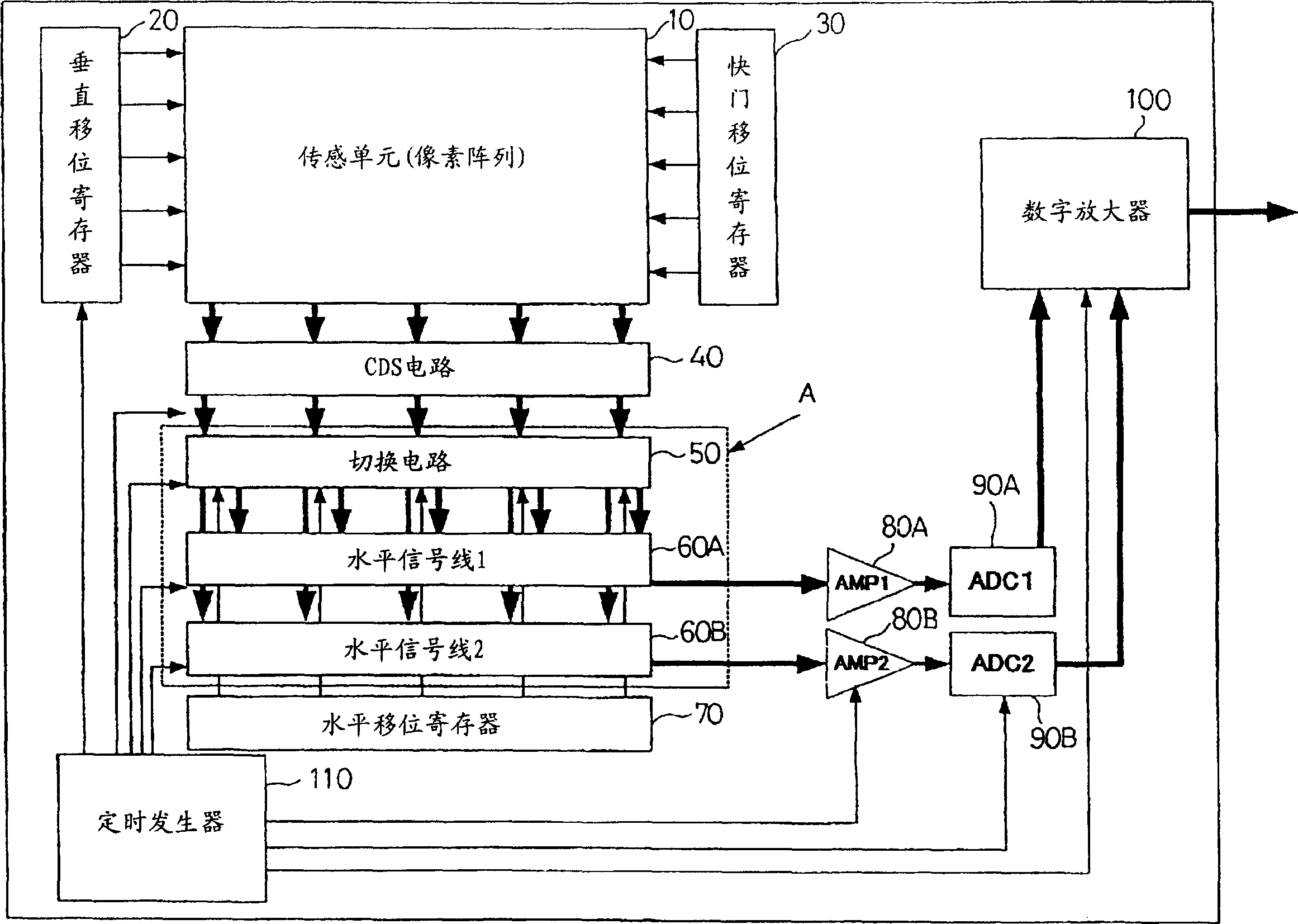
[0025] figure 1 is a block diagram illustrating the structure of a CMOS sensor according to an embodiment of the present invention.

[0026] Such as figure 1 As shown, the CMOS sensor according to this embodiment includes a sensing unit (pixel array) 10, a vertical shift register 20, a shutter shift register 30, a correlated double sampling (CDS) circuit 40, a switching circuit 50, horizontal signal lines 60A and 60B, horizontal shift register 70 , amplification circuits 80A and 80B, A / D converters 90A and 90B, digital amplifier 100 , and timing generator 110 .

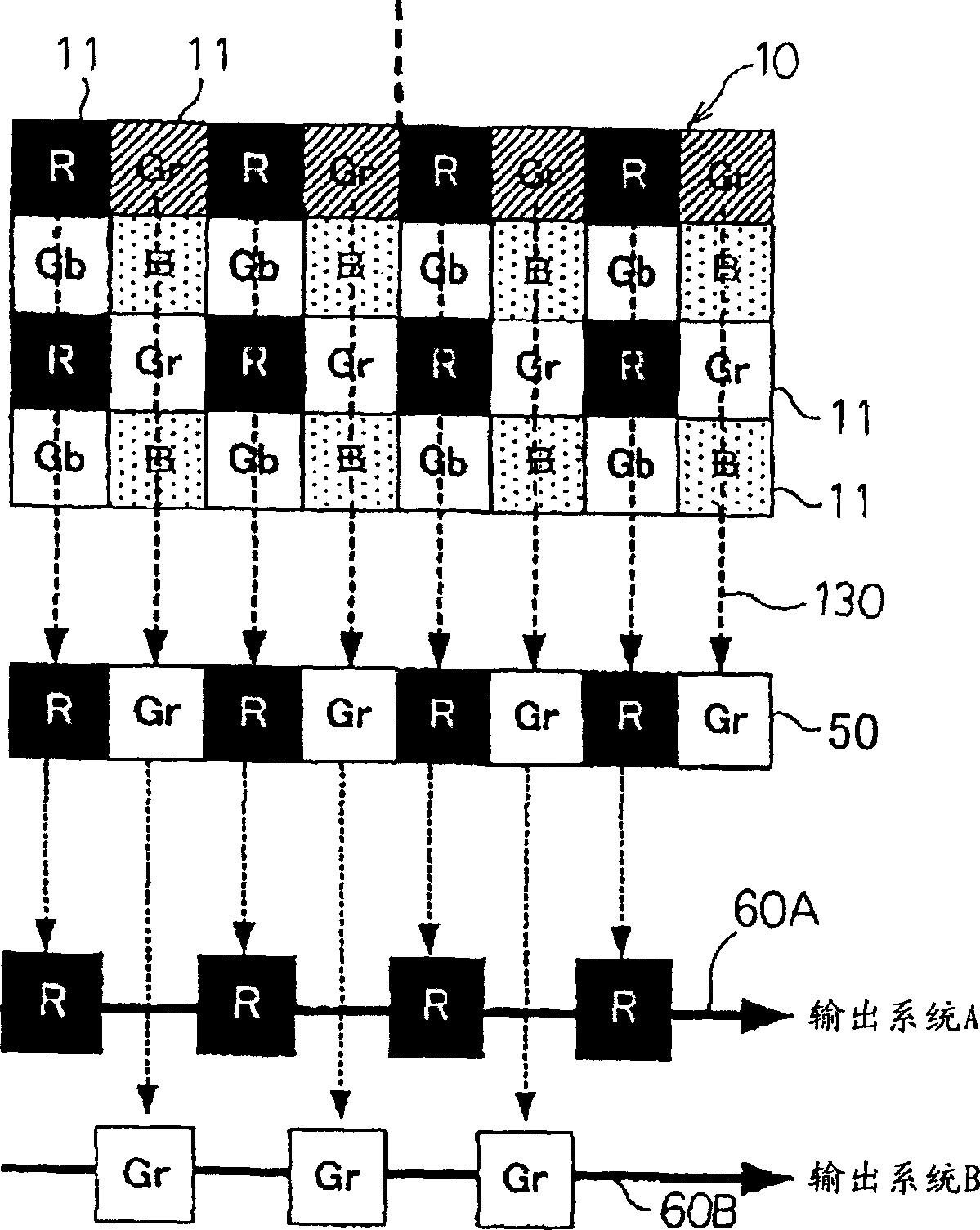
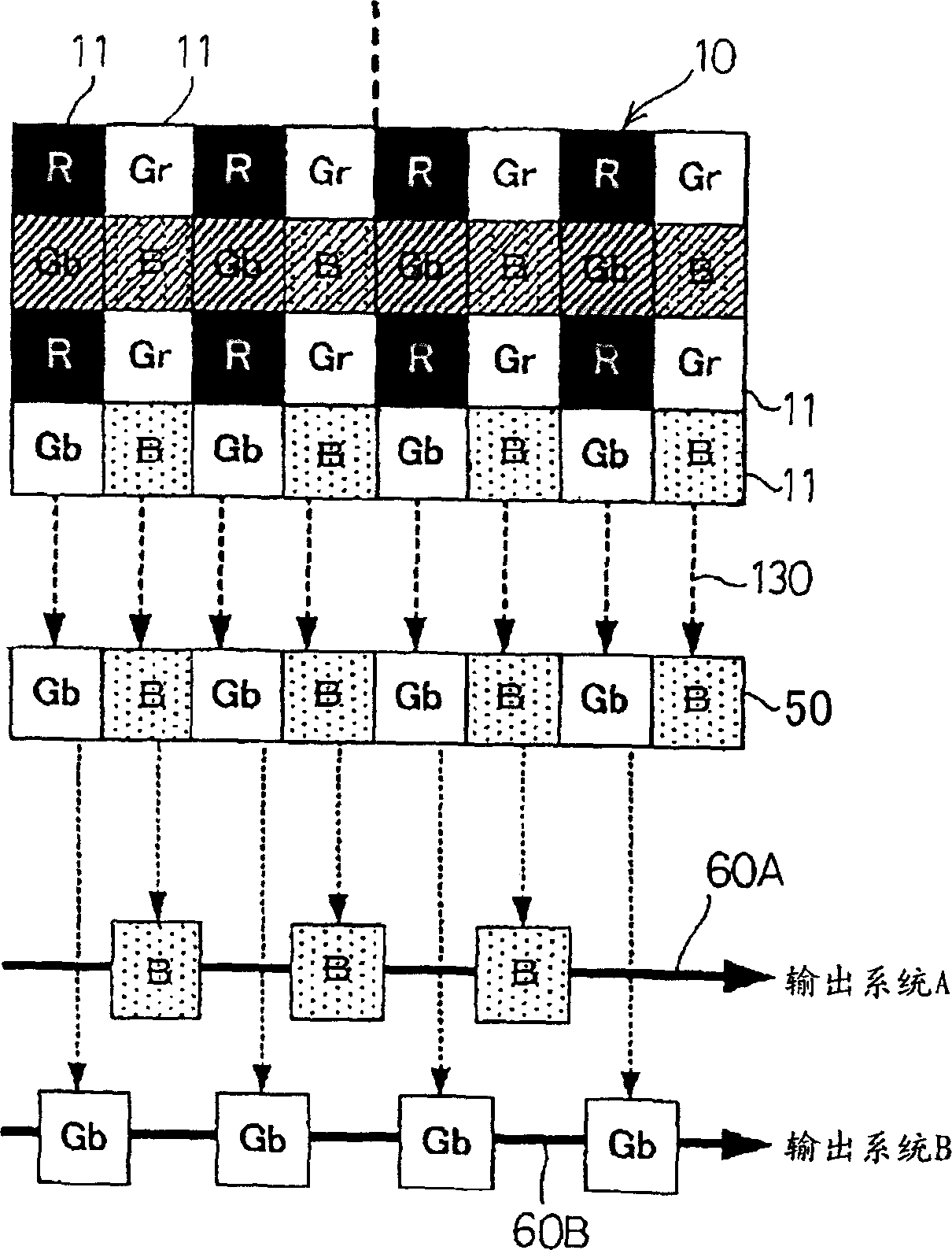
[0027] The sensing unit 10 includes pixels in a two-dimensional array. Each pixel includes a photoelectric transducer such as a photodiode and various types of pixel transistors. The sensing unit 10 converts signal charges generated in photoelectric transducers in pixels into electrical signals throug...


PUM


Abstract

In an arrangement where a plurality of horizontal signal lines are used to distribute pixel signals so as to realize a high speed operation, color differences and moire occurring in image signals are eliminated. It is shown that the pixel signals of a 2n-th row are being read out, and R pixels of the odd-numbered columns are outputted from a horizontal signal line (60A) to an output system (A). Meanwhile, Gr pixels of the even-numbered columns are outputted from a horizontal signal line (60B) to an output system (B). It is also shown that pixel signals of a 2n+1-th row are being read out, and Gb pixels of the odd-numbered columns are outputted from the horizontal signal line (60B) to the output system (B) via a switching operation of a switch circuit part (50). Similarly, the B pixels of the even-numbered columns are outputted from the horizontal signal line (60A) to the output system (A) via a switching operation of the switch circuit part (50).

Description

technical field [0001] The present invention relates to a solid-state imaging device such as a CMOS sensor that outputs a color image, and a method for reading a signal from the device. Background technique [0002] In general, a CMOS sensor is a solid-state imaging device that includes a two-dimensional pixel array of pixels. Each pixel includes: a photoelectric transducer for generating signal charges in response to incident light beams; and a pixel transistor for converting the signal charges into electric signals and outputting the electric signals. The CMOS sensor reads individual pixel signals through a plurality of vertical signal lines provided corresponding to columns of pixels, and processes the read pixel signals to output the processed signals to an output unit through horizontal signal lines. [0003] The CMOS sensor can randomly access individual pixels by selectively scanning pixels and signal processing circuits. [0004] Color filters with a predetermined ...

Claims


Application Information

Patent Timeline
Patent Type & Authority Applications(China)
IPC IPC(8): H04N9/07H01L27/146H04N5/335H04N5/341H04N5/365H04N5/369H04N5/374H04N9/04
CPCH04N9/045H04N25/447H04N25/134H04N25/78
Inventor 和田孝政船津英一马渕圭司中岛健阿部高志梅田智之中村信男藤田博明佐藤弘树
Owner SONY SEMICON SOLUTIONS CORP
Why Eureka
Eureka Blog
Learn More