Field emission device cathode device, its manufacture method and apparatus containing the device
A field emission device, cathode technology, applied in cold cathode manufacturing, electron emission electrode/cathode, electrode system manufacturing, etc., can solve problems such as separation of CNT fibers
Inactive Publication Date: 2010-11-10
SAMSUNG ELECTRONICS CO LTD
View PDF3 Cites 0 Cited by
- Summary
- Abstract
- Description
- Claims
- Application Information
AI Technical Summary
Problems solved by technology
Therefore, if the CNT fibers are to be sprinkled on a substrate and then coated, there will still be the problem of separating the CNT fibers for improved emission
Method used
View moreImage
Smart ImageViewing Examples
Examples
Embodiment 1
Embodiment 2
Embodiment 3
Login to View More PUM
| Property | Measurement | Unit |
|---|---|---|
| thickness | aaaaa | aaaaa |
| length | aaaaa | aaaaa |
| diameter | aaaaa | aaaaa |
Abstract
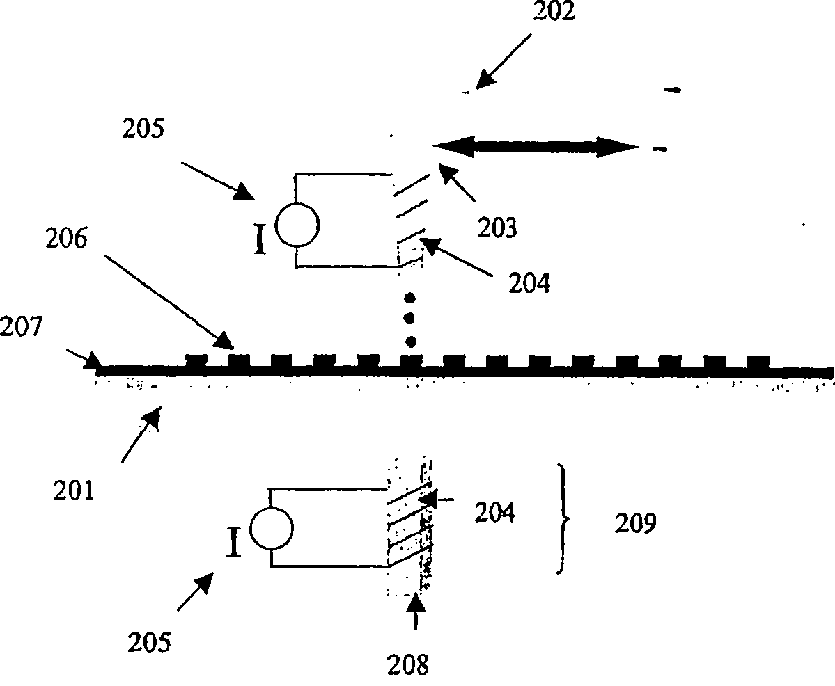
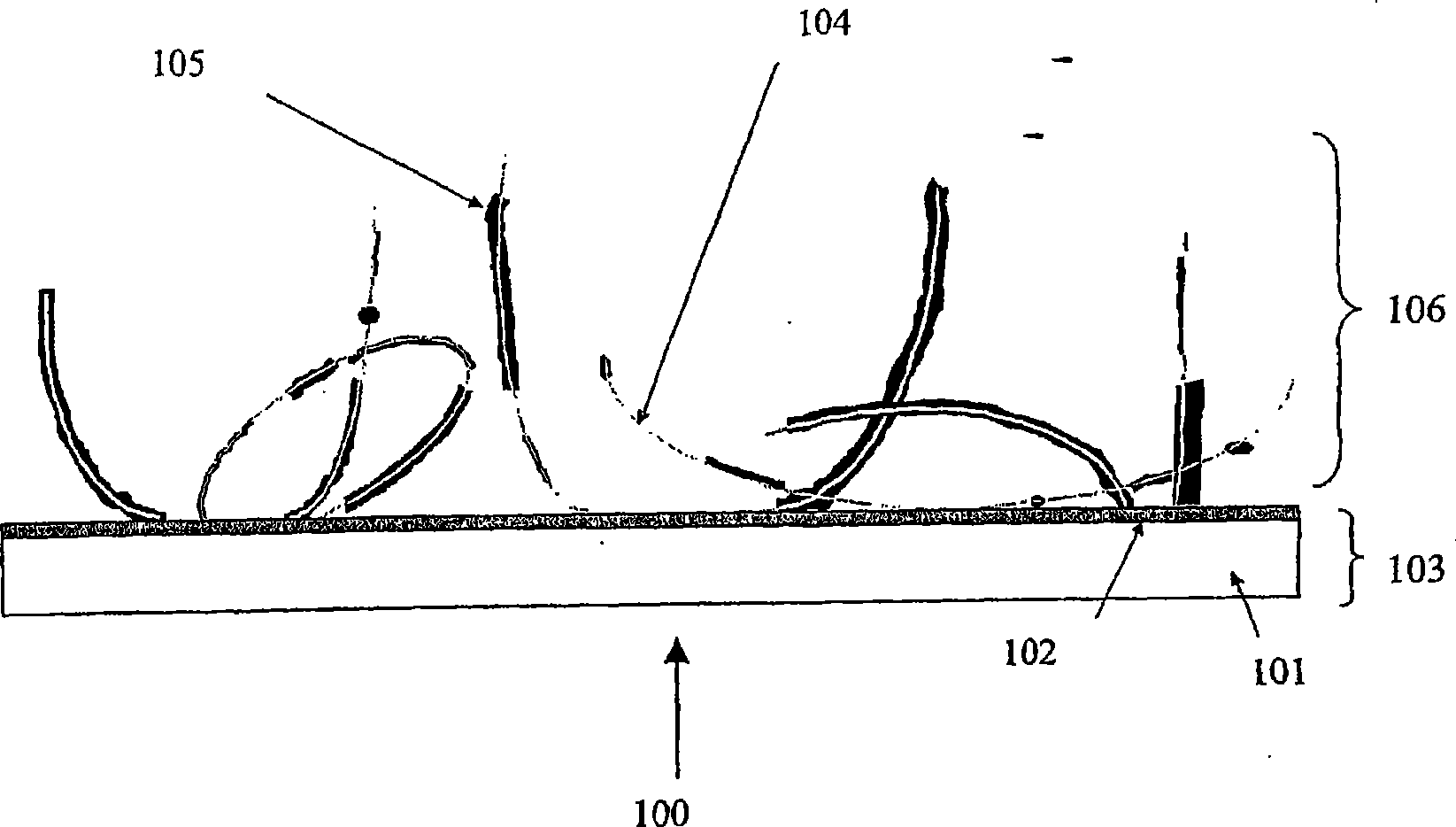
The present invention is directed towards metallized carbon nanotubes, methods for making metallized carbon nanotubes using an electroless plating technique, methods for dispensing metallized carbon nanotubes onto a substrate, and methods for aligning magnetically-active metallized carbon nanotubes. The present invention is also directed towards cold cathode field emitting materials comprising metallized carbon nanotubes, and methods of using metallized carbon nanotubes as cold cathode field emitters.
Description
Cathode device for field emission device, method for manufacturing same, and device containing same technical field The present invention relates generally to nanostructured materials, and more particularly to modified carbon nanotubes for field emission applications. Background technique Carbon nanotubes (CNTs) are currently being investigated for use as cold electron sources in various applications. These uses include displays, microwave sources, X-ray tubes, etc. For CNTs to be used as cold cathodes, they must be placed on a conductive surface (either a conductive substrate or a conductive film on a non-conductive substrate). Someone put the catalyst on the surface of the substrate and used CVD technology to grow carbon nanotubes in situ (Kimetal., J.Appl.Phys., 90(5), 2591(2001)). However, this has several drawbacks. This technique usually grows multi-walled carbon nanotubes (MWNTs), however, compared with single-walled carbon nanotubes (SWNTs), MWNTs have poor fiel...
Claims
Login to View More Application Information
Patent Timeline
 Patent Type & Authority Patents(China)
IPC IPC(8): H01J1/14H01J1/146H01J1/30H01J1/304H01J19/06H01J9/00H01J9/02B82B1/00C23C18/16C23C18/18C23C18/31H01J29/04H01J31/12
CPCB82Y10/00C23C18/31H01J9/025H01J2201/30469C23C18/1644B82B3/00B82Y25/00
Inventor D·毛Z·雅尼弗R·L·菲因克
Owner SAMSUNG ELECTRONICS CO LTD
- R&D Engineer
- R&D Manager
- IP Professional
Why Eureka
- Industry Leading Data Capabilities
- Powerful AI technology
- Patent DNA Extraction
Eureka Blog
Learn More Browse by: Latest US Patents, China's latest patents, Technical Efficacy Thesaurus, Application Domain, Technology Topic, Popular Technical Reports.
© 2024 PatSnap. All rights reserved.Legal|Privacy policy|Modern Slavery Act Transparency Statement|Sitemap|About US| Contact US: help@patsnap.com


