Gated fabrication of nanostructure field emission cathode material within a device

a nanostructure and cathode material technology, applied in the field of gated field emission cathode materials within a device, can solve the problems of reducing the work of gated cathode structures using these materials as fe elements, affecting the construction of fe devices, and reducing the work of gated cathode structures

Inactive Publication Date: 2005-02-22
UT BATTELLE LLC
View PDF4 Cites 51 Cited by
  • Summary
  • Abstract
  • Description
  • Claims
  • Application Information

AI Technical Summary

Problems solved by technology

However, very little work has been presented on integrated gated cathode structures using these materials as FE elements.
While all of these devices possess operating characteristics desirable in any FE device (i.e., low Eto and high brightness) these fabrication processes offer no way to precisely control the factors of location, orientation, shape or density of the emission sites.
These factors complicate the construction of FE devices that produce a well-focused electron beam as required in applications such as electron microscopy or electron beam lithography.
Another problem with this technology has been the need to use lithography equipment with sophisticated alignment capabilities.
Equipment with these capabilities is expensive.
The use of this equipment also requires time for the alignment function to be completed, thereby further adding to the overall cost of fabrication.

Method used


Image

  • Gated fabrication of nanostructure field emission cathode material within a device
  • Gated fabrication of nanostructure field emission cathode material within a device
  • Gated fabrication of nanostructure field emission cathode material within a device

Examples


example 1

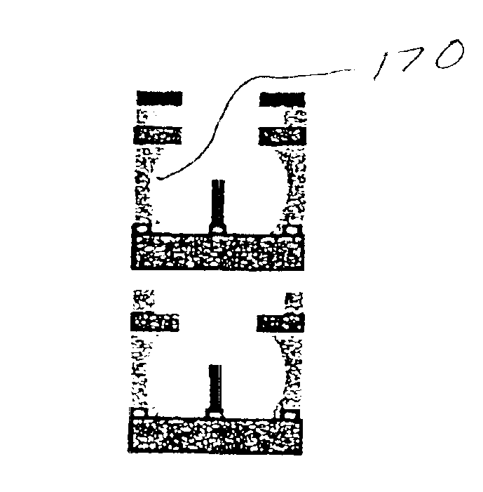
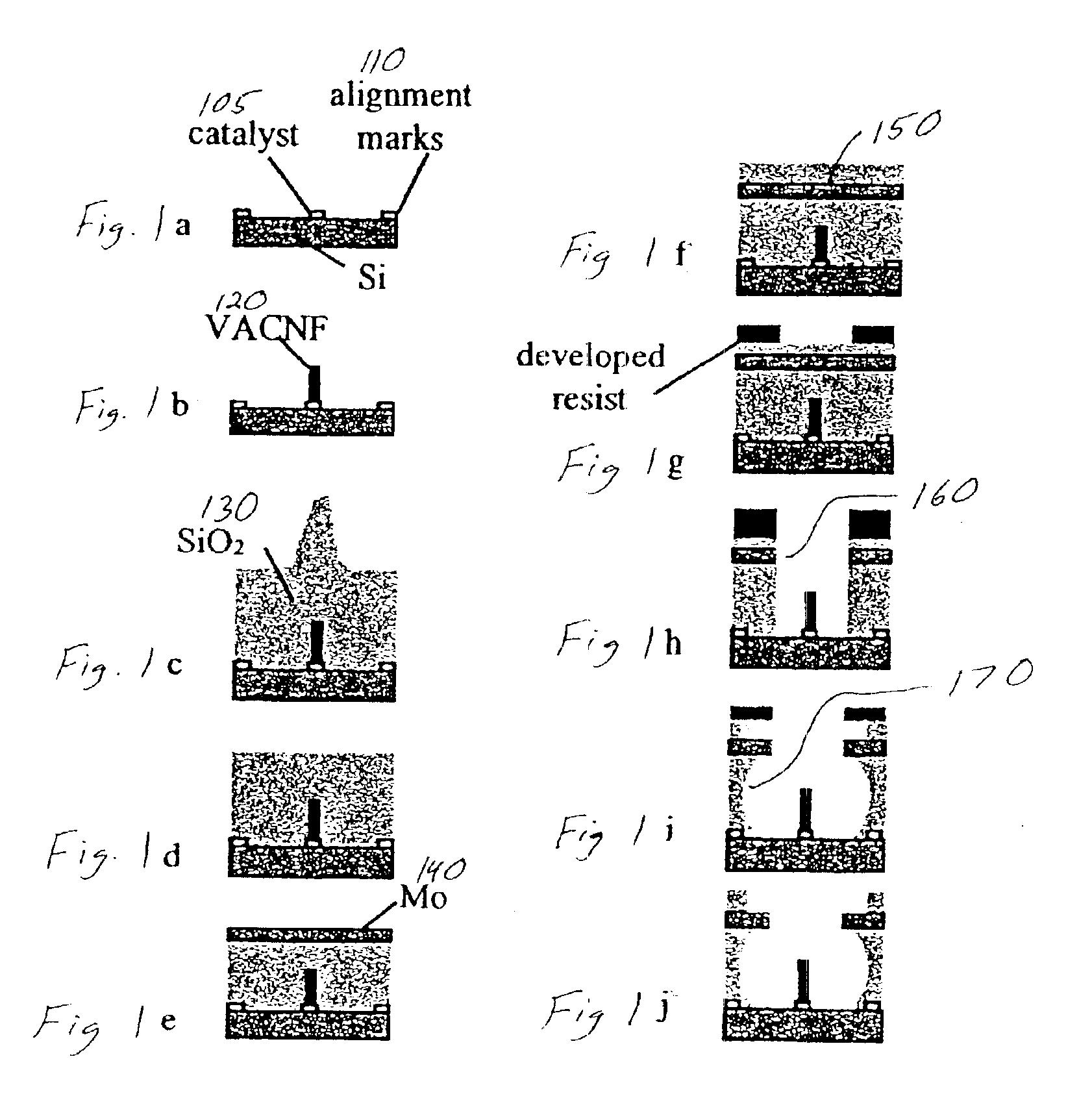
[0064]FIGS. 1A-1J depict a process flow for fabrication of the gated cathode structures. Three-inch diameter low resistivity n-type Si wafers were used as substrates throughout this example. Prior to performing processing, the substrates were cleaned in a solution of ammonium fluoride and hydrofluoric (HF) acid 6:1 for 60 s to remove native oxide from the substrate surface. Immediately following this cleaning, the substrates were spin coated with a bilayer of polymethyl methacrylate (PMMA, MicroChem, Nano PMMA). The bilayer consisted of two different molecular weight PMMA formulations to produce an undercut in the developed resist sidewall profile to facilitate liftoff pattern transfer. The lower layer was a 4% 495K PMMA in anisole spun onto each substrate at 4000 rpm for one minute to produce a 1000 Å thick layer. Following spin coating, each substrate was baked for 15 minutes on a 170° C. hotplate. After removing the substrates from the hotplate, a layer of 2% 950 k PMMA in methyl...

example 2

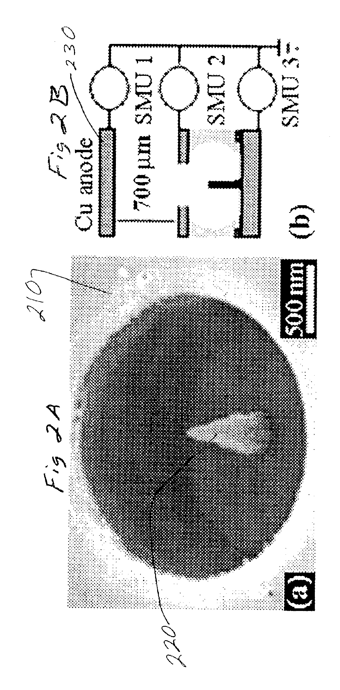
[0080]A schematic diagram of a different device fabrication process for the gated cathode structures is shown in FIGS. 7A-7I. Whole 3″ or 4″ low resistivity n-type Si wafers were used as substrates throughout this example. Conventional high-resolution electron beam lithography (EBL) and liftoff pattern transfer was used to define catalyst site(s) 710 for deterministic growth of VACNF and alignment marks for subsequent lithographic patterning processes (see FIG. 7A). The catalyst site pattern consisted of 100-nm diameter circles. These patterns were metallized with 100 Å of Ti followed by 100 Å of Ni deposited by electron beam physical vapor deposition (PVD). The Ti layer was deposited between the Ni catalyst and Si substrate to prevent catalyst silicide formation at the moderately high growth temperature of approximately 700° C. The wafers were mounted directly on a heated cathode inside the PECVD growth system. After evacuating the growth system to a suitable base pressure, the tem...

example 3

[0082]A schematic diagram of a self aligned fabrication process for the gated cathode structures is shown in FIGS. 9A-9F. In this example, whole 3″ low resistivity Si n-type wafers were used as substrates. Electron beam lithography and physical vapor deposition (PVD) were used to realize the catalyst site(s) 910 for VACNF growth and alignment marks for subsequent lithographic patterning (see FIG. 9A). DC plasma enhanced chemical vapor deposition (PECVD) of VACNF material 920 was performed at 700° C. (see FIG. 9B). This process produced VACNF that were 1-μm tall on average with tip diameters of less than 30 nm. A 1.2 μm thick layer of SiO2 930 was deposited onto the substrates using a silane-based rf PECVD process and resulted in the formation of conformal mounds surrounding the VACNF emitters (see FIG. 9C). The gate electrode 940 was defined using photolithography, omitting any lithographic definition of apertures aligned to the VACNF emitters. The gate pattern was metallized with 5...


PUM

PropertyMeasurementUnit
diameteraaaaaaaaaa
oblique angle micrographsaaaaaaaaaa
diameteraaaaaaaaaa

Abstract

Gated field emission devices and systems and methods for their fabrication are described. A method includes growing a substantially vertically aligned carbon nanostructure, the substantially vertically aligned carbon nanostructure coupled to a substrate; covering at least a portion of the substantially vertically aligned carbon nanostructure with a dielectric; forming a gate, the gate coupled to the dielectric; and releasing the substantially vertically aligned carbon nanostructure by forming an aperture in the gate and removing a portion of the dielectric.

Description

CROSS-REFERENCE TO RELATED APPLICATION[0002]This application is related to and claims a benefit of priority under 35 U.S.C. 119(e) from U.S. Ser. No. 60 / 293,780, filed May 25, 2001, (ID No. 0960, S-96,723), the entire contents of which are hereby expressly incorporated by reference for all purposes.STATEMENT AS TO RIGHTS TO INVENTIONS MADE UNDER FEDERALLY-SPONSORED RESEARCH OR DEVELOPMENT[0003]This invention was made with United States Government support under contract No. 1868HH26X1 to UT-Battelle, L.L.C. awarded by DARPA. The Government has certain rights in this invention.BACKGROUND OF THE INVENTION[0004]1. Field of the Invention[0005]The invention relates generally to the field of electron emitting devices. More particularly, the invention relates to gated field emission devices.[0006]2. Discussion of the Related Art[0007]Field emission (FE) of electrons from nanostructured graphitic carbon-based materials including single-1-3 and multi-walled4,5 carbon nanotubes (CNT) and carbo...

Claims


Application Information

Patent Timeline
Patent Type & Authority Patents(United States)
IPC IPC(8): H01J9/02B81C1/00
CPCB82Y10/00H01J9/025H01J2201/30469
Inventor GUILLOM, MICHAEL A.SIMPSON, MICHAEL L.MERKULOV, VLADIMIR I.MELECHKO, ANATOLI V.LOWNDES, DOUGLAS H.
Owner UT BATTELLE LLC
Why Eureka
Try Eureka