

LED with hot channel bonding layer
A technology of light-emitting diodes and bonding layers, applied in electrical components, circuits, semiconductor devices, etc., can solve the problems of small thermal conductivity, poor heat dissipation, and reduced thermal resistance and heat dissipation function luminous efficiency.
- Summary
- Abstract
- Description
- Claims
- Application Information
AI Technical Summary
Problems solved by technology
Method used
Image

Examples
Embodiment 1
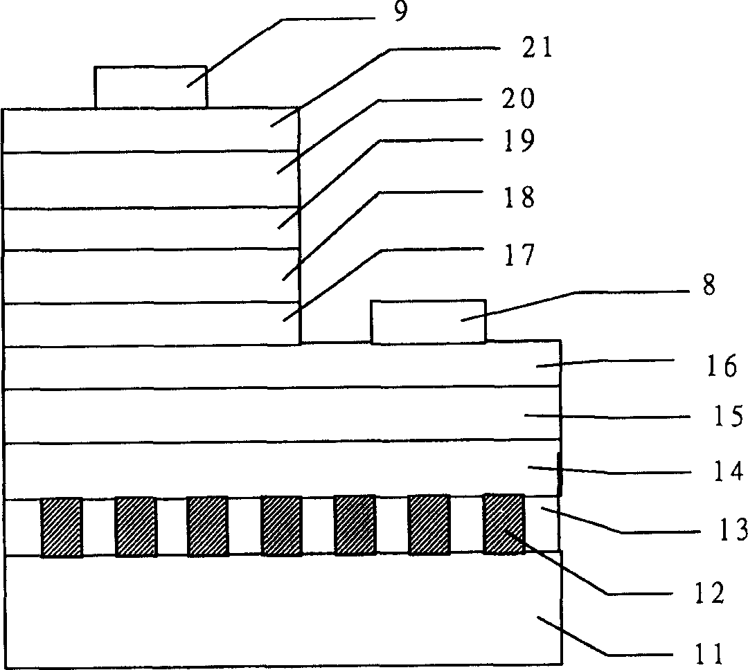
[0022] see figure 1 , according to a preferred embodiment of the present invention, a light-emitting diode with a thermal channel adhesive layer includes a high heat dissipation substrate 11, an adhesive layer 13 with a bump thermal channel 12 formed on the high heat dissipation substrate, wherein, through the bump Penetrating or partially penetrating through the adhesive layer to form a thermal channel, a reflective layer 14 formed on the adhesive layer with a bump thermal channel, an insulating layer 15 formed on the reflective layer, and an insulating layer formed on the insulating layer A transparent conductive layer 16, wherein the upper surface of the transparent conductive layer includes a first surface area and a second surface area, a first contact layer 17 formed on the first surface area, a first contact layer 17 formed on the first contact A first confinement layer 18 on the layer, a luminous layer 19 formed on the first confinement layer, a second confinement laye...
Embodiment 2
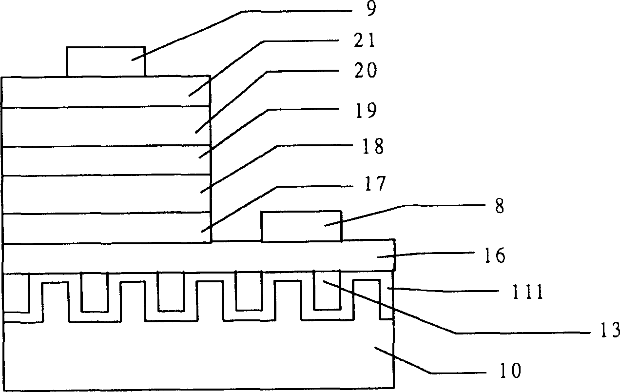
[0024] see figure 2 According to another preferred embodiment of the present invention, a bonded light-emitting diode with thermal channels includes a high heat dissipation substrate 10 with bump thermal channels, an insulating layer 111 formed on the high heat dissipation substrate with bump thermal channels, formed on The bonding layer 13 on the insulating layer is used to make the insulating layer penetrate or partially penetrate the bonding layer through bumps, and a transparent conductive layer 16 formed on the insulating layer and the bonding layer, wherein the upper surface of the transparent conductive layer Comprising a first surface region and a second surface region, a first contact layer 17 formed on the first surface region, a first confinement layer 18 formed on the first contact layer, formed on the first A light-emitting layer 19 on a binding layer, a second binding layer 20 formed on the light-emitting layer, a second contact layer 21 formed on the second bin...
Embodiment 3
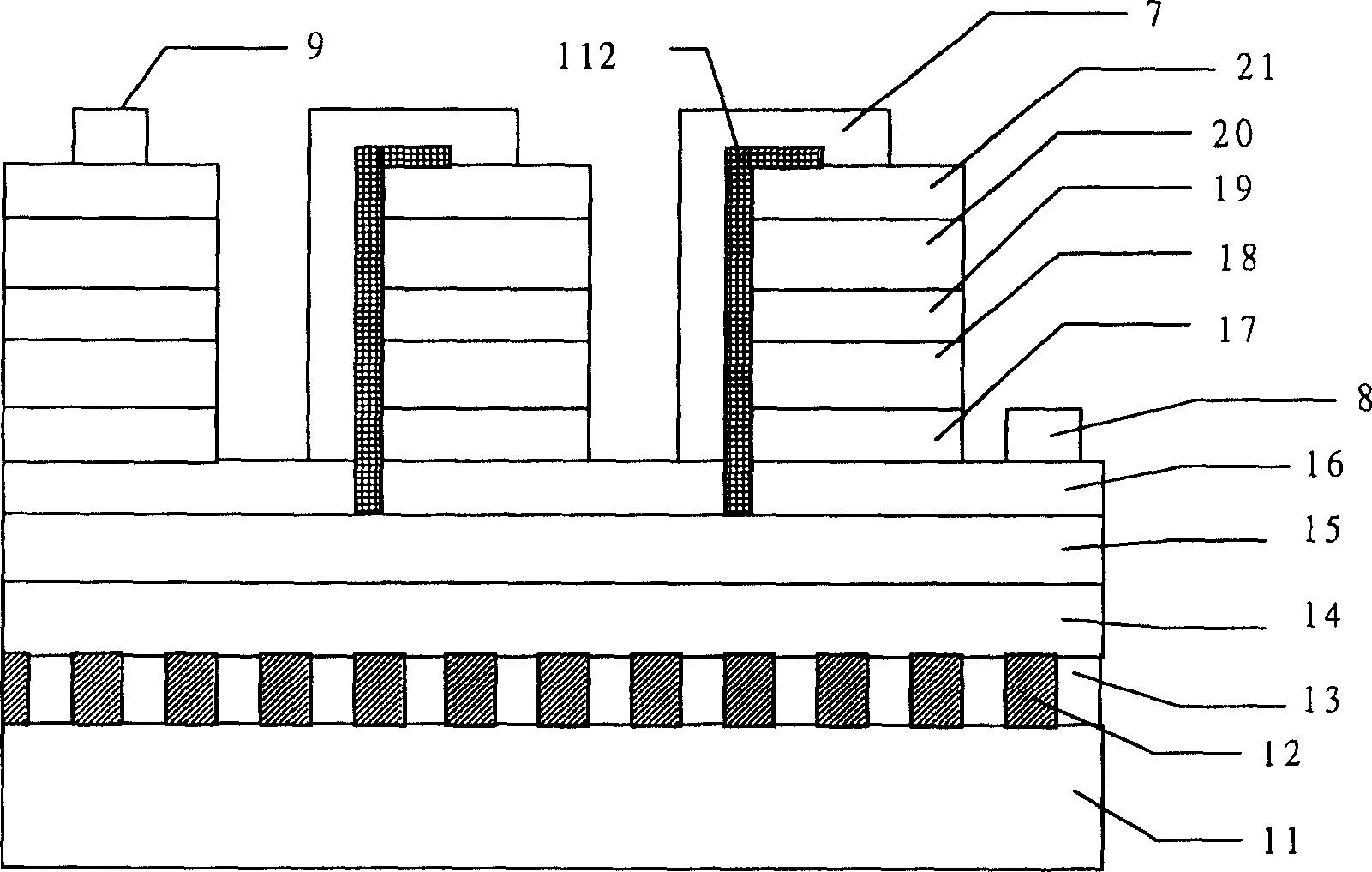
[0026] see image 3 , according to yet another preferred embodiment of the present invention, a bonded light-emitting diode array with thermal channels, which is compatible with figure 1 Similar to the first preferred embodiment, the difference is that the upper surface of the insulating layer 15 includes a plurality of first surface regions and a plurality of second surface regions, and a plurality of transparent transparent layers formed on the plurality of first surface regions of the insulating layer Conductive layer 16, the plurality of transparent conductive layers have a plurality of first surface areas and a plurality of second surface areas, and a plurality of LED stacks formed on the plurality of first surface areas of the plurality of transparent conductive layers, The LED stack sequentially includes a first contact layer 17, a first confinement layer 18, a light emitting layer 19, a second confinement layer 20, a second contact layer 21, formed on the second surfac...
PUM
 Abstract
Description
Claims
Application Information