Compound semiconductor device and manufacturing method thereof

A manufacturing method and semiconductor technology, applied in the direction of semiconductor/solid-state device manufacturing, semiconductor devices, semiconductor/solid-state device components, etc., can solve problems such as fixed deterioration, yield reduction, and reliability deterioration, so as to ensure insulation and finished products The effect of improving the rate and improving the characteristics

Inactive Publication Date: 2006-03-15
SANYO ELECTRIC CO LTD
View PDF2 Cites 3 Cited by
  • Summary
  • Abstract
  • Description
  • Claims
  • Application Information

AI Technical Summary

Problems solved by technology

[0025] Therefore, problems such as deteriorating the fixity of the joint or damaging the substrate occur, causing a decrease in yield or deterioration in reliability.

Method used


Image

  • Compound semiconductor device and manufacturing method thereof
  • Compound semiconductor device and manufacturing method thereof
  • Compound semiconductor device and manufacturing method thereof

Examples


Embodiment Construction

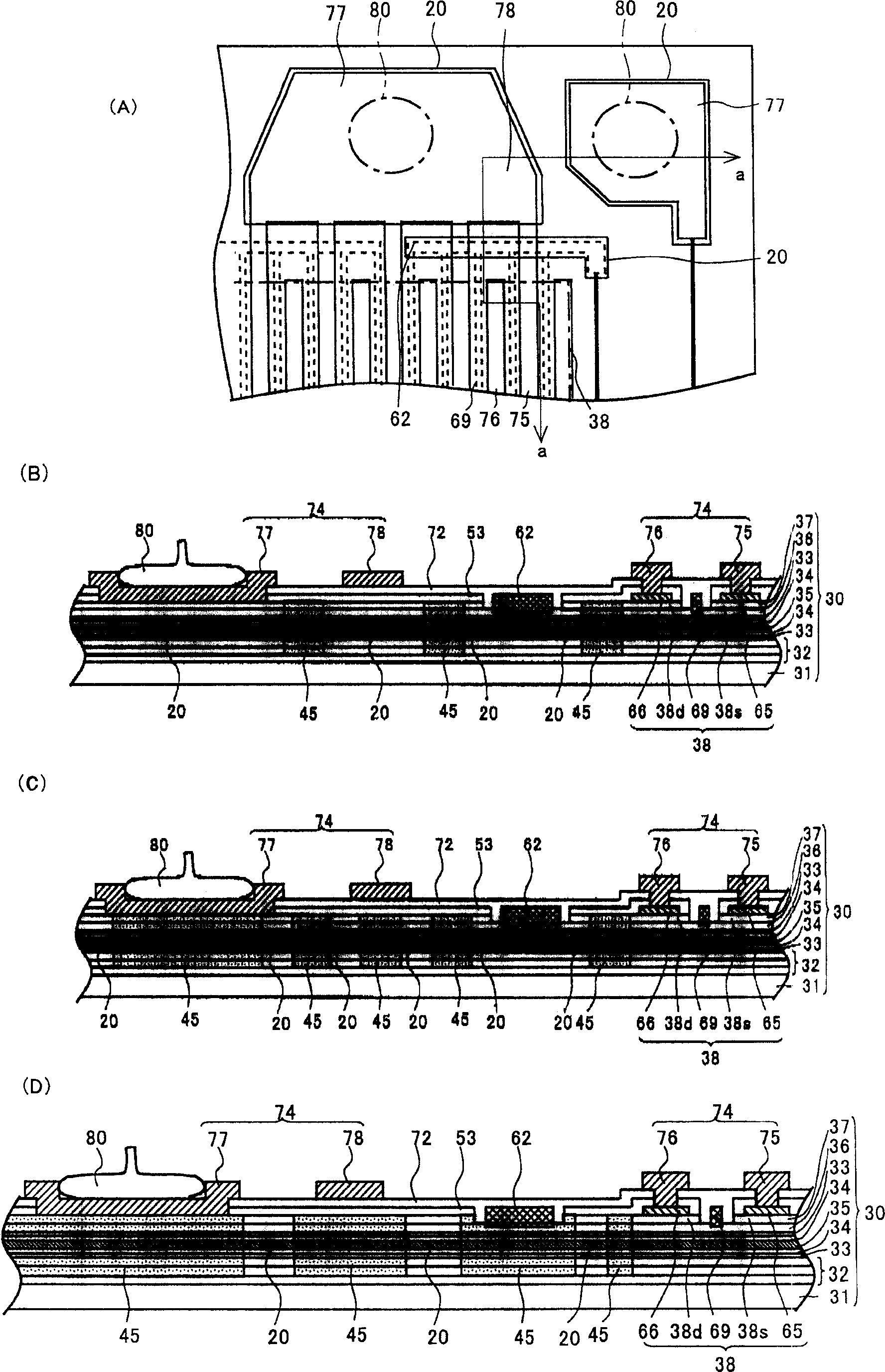
[0101] Refer below Figure 1 to Figure 8 Embodiments of the present invention will be described, and the configuration will be described as an example. Figure 9 A HEMT (High Electron Mobility Transistor: High Electron Mobility Transistor) such as a switch circuit device (SPDT), electrode pads, and wiring portions are shown.

[0102] figure 1 is a diagram showing an example of the compound semiconductor device of this embodiment, figure 1 (A) is a floor plan, figure 1 (B) is a-a line sectional view. In addition, the same symbols are used for the same constituent elements as in the prior art.

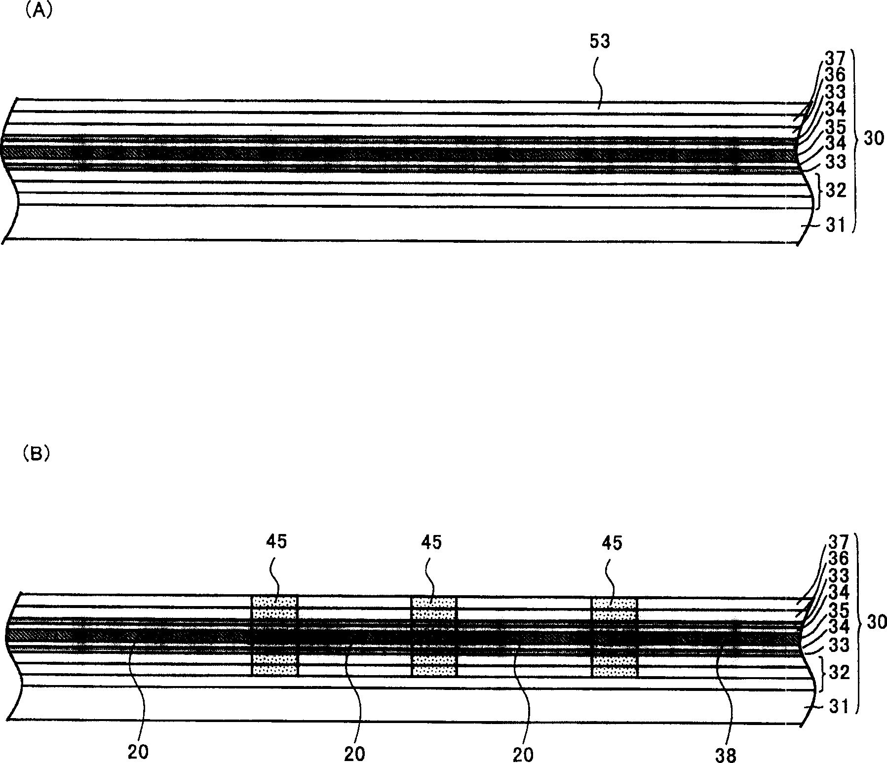
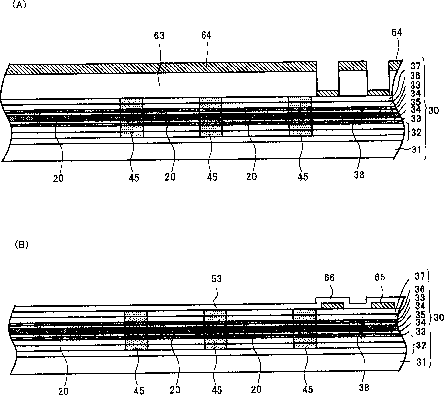
[0103] Such as figure 1(A), (B), method of forming the substrate 30 Firstly, the non-doped buffer layer 32 is laminated on the semi-insulating GaAs substrate 31 . The buffer layer is often formed from multiple layers. Then, an n+ type AlGaAs layer 33 as an electron supply layer, an undoped InGaAs layer 35 as an electron transit layer, and an n+ type AlGaAs layer 33 as an electr...


PUM


Abstract

A pad electrode of a high electron mobility transistor is formed solely of a pad metal layer without providing a gate metal layer. A high concentration impurity region is provided below the pad electrode, and the pad electrode is directly contacted to a substrate. Predetermined isolation is ensured by the high concentration impurity region. Accordingly, in a structure not requiring a nitride film as similar to the conventional art, it is possible to avoid defects upon wire boding attributing to hardening of the gate metal layer. Therefore, even in the case of a buried gate electrode structure for enhancing characteristics of the high electron mobility transistor, it is possible to enhance reliability and yields.

Description

technical field [0001] The present invention relates to a compound semiconductor device and a method for manufacturing the same, and more particularly, to a compound semiconductor device and a method for manufacturing the compound semiconductor device that improves FET characteristics and reduces defects during wire bonding. Background technique [0002] Microwaves in the GHz band are often used in mobile communication devices such as mobile phones, and switching elements for switching these high-frequency signals are often used in switching circuits for antennas and switching circuits for transmitting and receiving signals (for example, JP-A-9-181642). As this element, field-effect transistors (hereinafter referred to as FETs) using gallium-arsenic (GaAs) are often used because they must handle high frequencies. Accordingly, monolithic microwave integrated circuits that integrate the above-mentioned switching circuits themselves are being developed. (MMIC) development. [...

Claims


Application Information

Patent Timeline
Patent Type & Authority Applications(China)
IPC IPC(8): H01L29/80H01L23/52H01L21/3205H01L21/336H01L21/338H01L21/60H01L21/768H01L21/822H01L23/485H01L23/522H01L27/04H01L27/06H01L27/095H01L29/778H01L29/812H01L31/0328H01L31/0336H01L31/072H01L31/109
CPCH01L2924/01015H01L2224/05669H01L2924/01023H01L2924/01082H01L2924/00014H01L2924/01004H01L24/05H01L29/7785H01L2924/30105H01L2224/48644H01L2224/05666H01L2224/48666H01L2924/01022H01L2924/01028H01L2924/30107H01L2924/1423H01L24/48H01L2224/05644H01L27/0605H01L24/03H01L24/45H01L2224/48599H01L2924/19043H01L2924/05042H01L2924/10336H01L2924/01079H01L2224/48463H01L2224/04042H01L2924/14H01L2924/01005H01L2924/01033H01L2924/01006H01L2924/10329H01L2924/01078H01L2224/05599H01L2924/01042H01L2924/01014H01L2224/45144H01L2224/48669H01L2924/01031H01L2924/13064H01L2924/1306H01L2924/12032H01L2924/181H01L2924/01032H01L2924/00H01L29/80
Inventor 浅野哲郎
Owner SANYO ELECTRIC CO LTD
Why Eureka
Try Eureka