Method for producinfg self luminous panel

A manufacturing method and self-illumination technology, applied in electroluminescent light sources, light sources, electric light sources, etc., can solve the problems of not being able to fully obtain the sealing effect of self-luminous components, reducing panel production efficiency, and defoaming

Inactive Publication Date: 2006-03-22
TOHOKU PIONEER CORP
View PDF4 Cites 3 Cited by
  • Summary
  • Abstract
  • Description
  • Claims
  • Application Information

AI Technical Summary

Problems solved by technology

[0014] If the self-luminous element (organic EL element) formed on the substrate is directly covered with a sealing material (sealing resin) as in the above-mentioned prior art, it is necessary to increase the number of substrates on which the self-luminous element is formed (hereinafter referred to as the element-side substrate). ) performs the process of coating the sealing material, so there is a problem that the production efficiency of the panel is lowered due to the increase of the manufacturing process of the element side substrate
[0015] Moreover, since the sealing material layer is formed on the self-luminous element formed on the substrate, it is difficult to perform degassing and other treatments on the sealing material before pasting the sealing substrate, so there is also a problem that the sealing effect on the self-luminous element cannot be fully obtained. The problem
[0016] In addition, it is difficult to control the coating range of the sealing resin before curing with high precision. In the method of manufacturing the organic EL display device described in Patent Documents 1 and

Method used


Image

  • Method for producinfg self luminous panel
  • Method for producinfg self luminous panel
  • Method for producinfg self luminous panel

Examples


Embodiment Construction

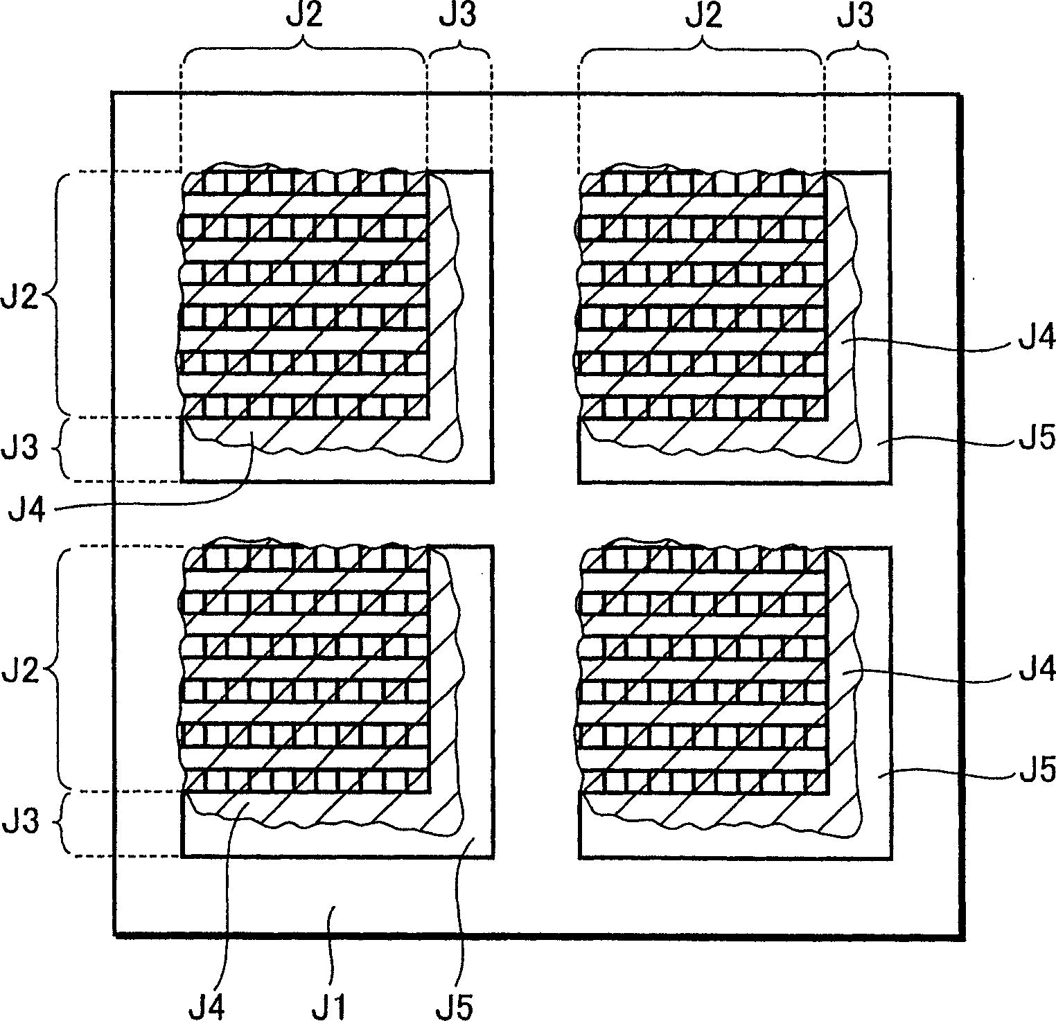
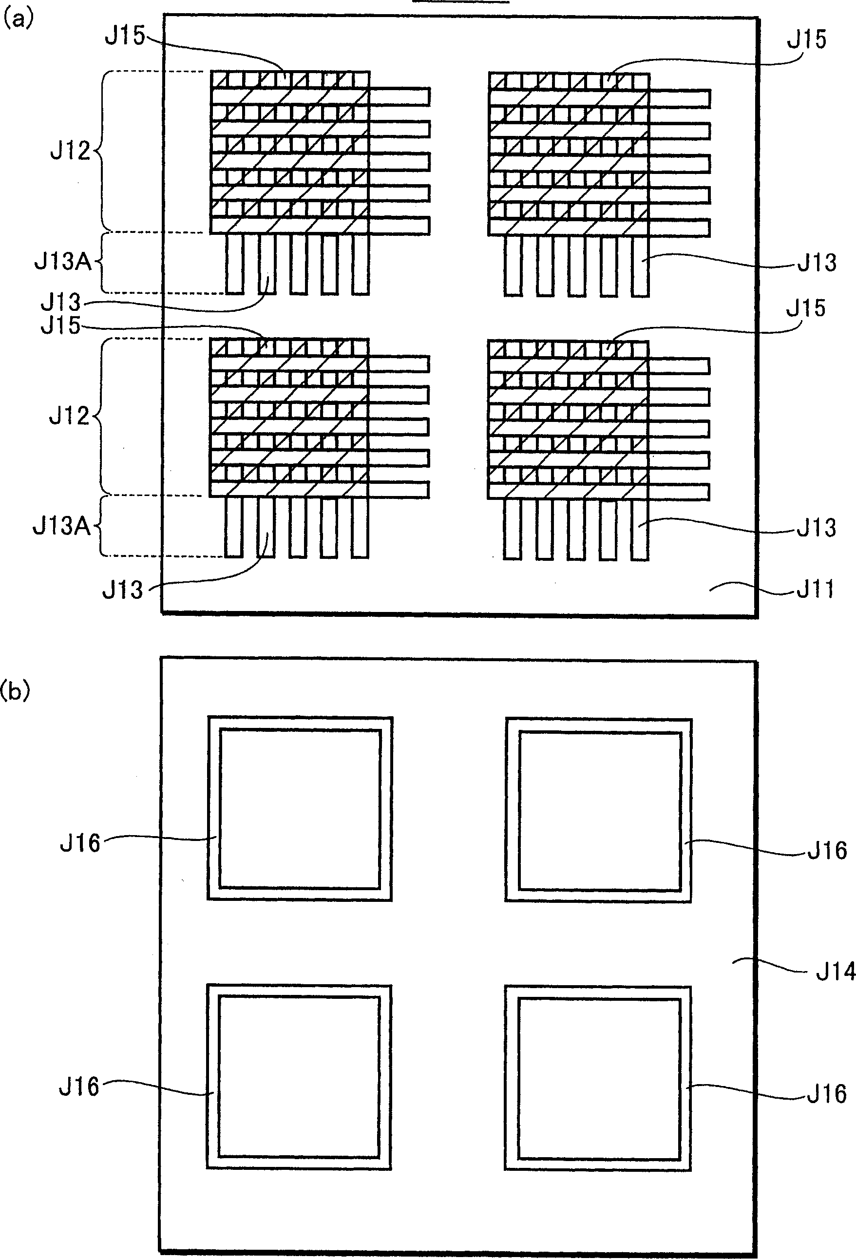
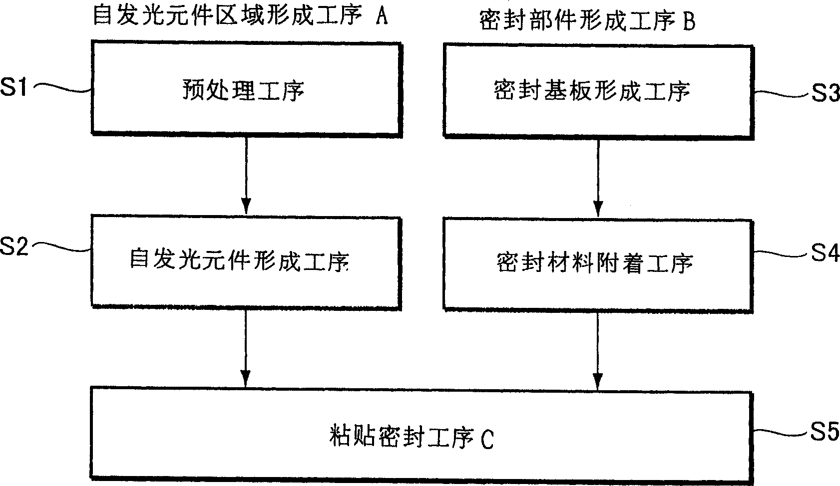
[0030] Hereinafter, embodiments of the present invention will be described with reference to the drawings. image 3 It is an explanatory drawing (flow chart) explaining the manufacturing method of the self-luminous panel which concerns on one Embodiment of this invention. The manufacturing method includes a self-light-emitting element region forming step A, a sealing member forming step B, and an adhering sealing step C.

[0031] Self-luminous element region formation process A: The substrate (element-side substrate) on which the self-luminous element is formed is subjected to the pretreatment process S1 (preparing the substrate, forming the lower electrode and the lead wiring pattern, forming the insulating film pattern, forming the cathode partition wall, cleaning the substrate, etc.) ), and a step (self-luminous element forming step) S2 including forming an organic layer including a light-emitting layer and an upper electrode, and forming a self-luminous element including a ...


PUM


Abstract

The invention provides a method of manufacturing a self-luminous panel using a sealing structure directly covering a self-luminous element on a substrate with sealing material, in which productivity of the panel is not made worse. A self-luminous element region forming process A and a luminous element region forming process B are independently performed. A substrate having a self-luminous element region formed thereon in the self-luminous element region forming process A and a seal substrate having a layer of sealing material formed thereon in the seal member forming process B are laminated to each other in a sealing process C. In the display region forming process A, the self-luminous element forming process is performed (S2) after a pretreatment process (S1). In the luminous element region forming process B, the sealing members are formed into the sizes of the sealing substrates respectively (S3) and then the sealing material is adhered on the sealing member (S4).

Description

technical field [0001] The invention relates to a method for manufacturing a self-luminous panel. Background technique [0002] Self-luminous panels represented by organic EL (electroluminescence) panels can be used in displays of mobile phones, flat-screen TVs, information terminals, etc., and are expected to be used in the interior of automotive function displays such as speedometers, etc. Panels, functional display parts for electrical appliances, film displays, outdoor guide displays, or lighting are being actively researched and developed. [0003] This kind of self-luminous panel is formed by arranging multiple or single self-luminous elements on a substrate. As self-luminous elements, in addition to organic EL elements, LEDs (light-emitting diodes), FEDs (electroluminescent displays), etc. light emitting element. [0004] The structure of the self-luminous element takes an organic EL element as an example. It is formed in such a way that an organic layer (including ...

Claims


Application Information

Patent Timeline
IPC IPC(8): G09F9/30H05B33/04H05B33/12
CPCH01L2924/12044H10K50/8426H10K50/84H10K71/00
Inventor 免田芳生
Owner TOHOKU PIONEER CORP
Why Eureka
Try Eureka