Display panel driving circuit and driving method

A display panel and drive circuit technology, applied in the direction of static indicators, instruments, etc., can solve the problems of response time difference, increase of resistance or electrostatic capacitance, inability to solve the unevenness of brightness, etc., and achieve the effect of correcting uneven brightness

Inactive Publication Date: 2006-04-19
OKI ELECTRIC IND CO LTD
View PDF1 Cites 135 Cited by
  • Summary
  • Abstract
  • Description
  • Claims
  • Application Information

AI Technical Summary

Problems solved by technology

[0006] However, even though the liquid crystal display device can compensate the color reproduction characteristics or optical response characteristics of the liquid crystal panel, as the display area of ​​the display panel increases, the resistance or sta

Method used


Image

  • Display panel driving circuit and driving method
  • Display panel driving circuit and driving method
  • Display panel driving circuit and driving method

Examples


Embodiment 1

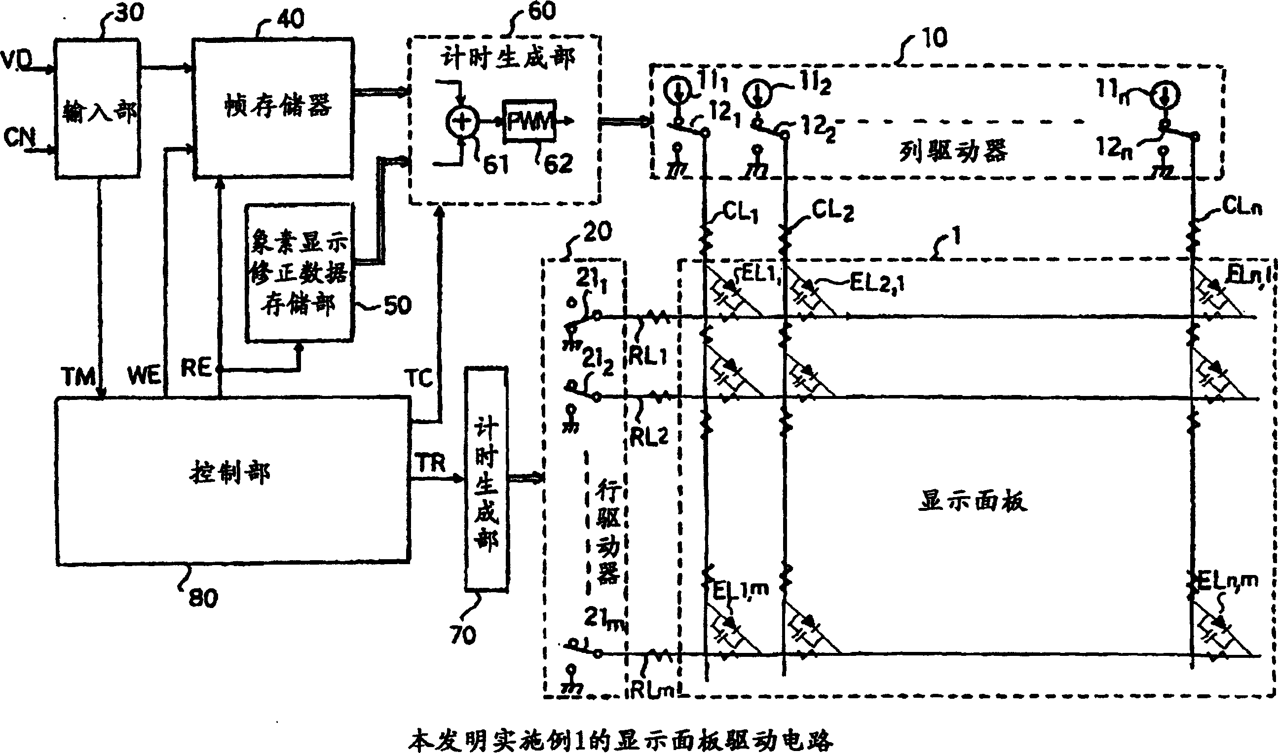
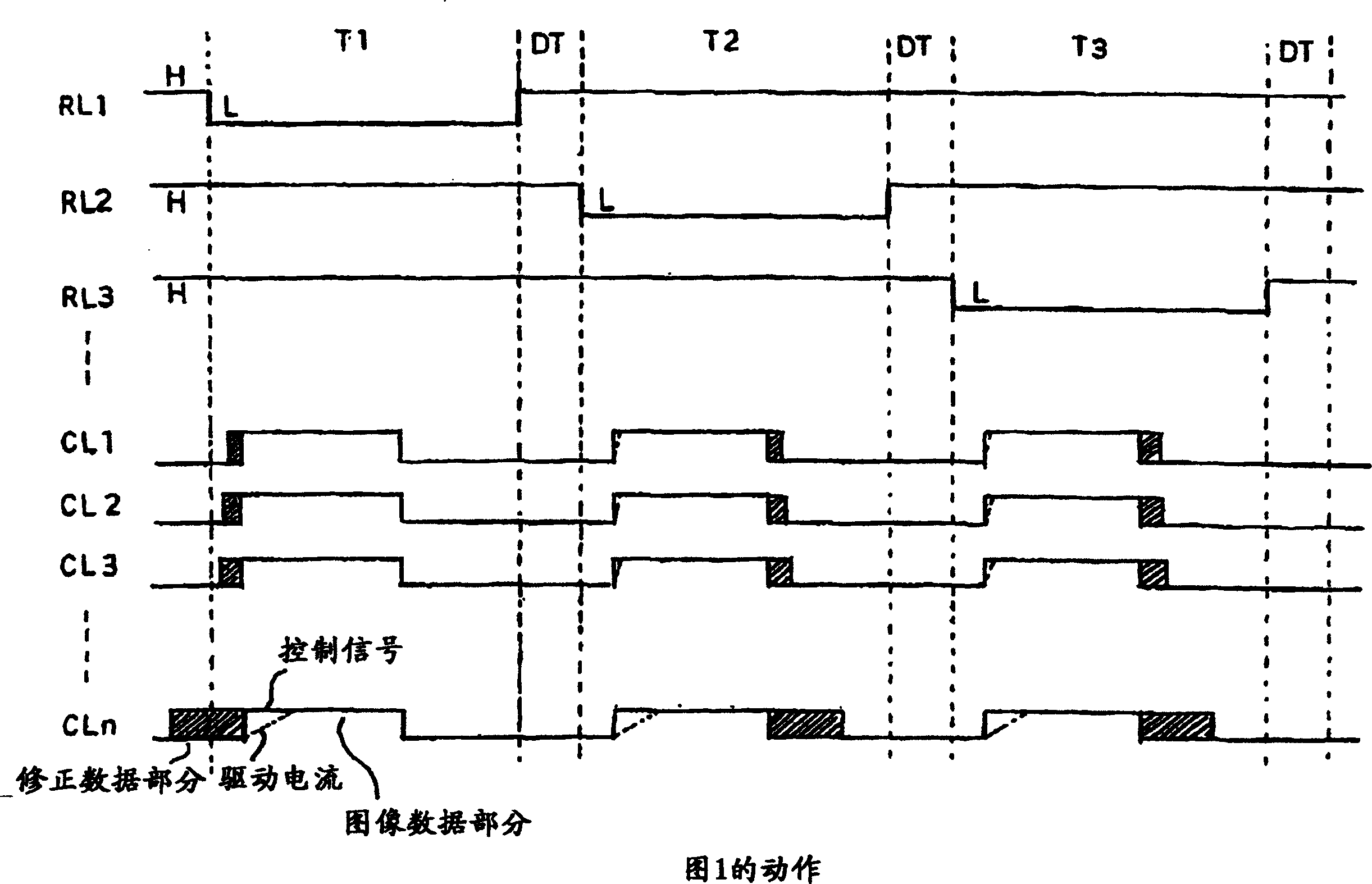
[0017] figure 1 It is a configuration diagram showing a display panel driving circuit according to Embodiment 1 of the present invention.

[0018] The display panel driving circuit has a column driver 10 and a row driver 20 for driving the display panel 1 . The display panel 1 is, for example, an organic EL panel, and has column lines CLi (i=1 to n) arranged in parallel at regular intervals and row lines RLj (j=1 to n) orthogonal to these column lines CLi and arranged in parallel at regular intervals. m). At each intersection of a column line CLi and a row line RLj, a light emitting element ELi,j is arranged.

[0019] In addition, although not a circuit element, in each of the column line CLi and the row line RLi, there is inevitably a distributed resistance component accompanying the wiring thereof. In addition, there must be electrostatic capacitance caused by the light emitting elements ELi,j provided between parallel column lines CLi, between row lines RLj, between inte...

Embodiment 2

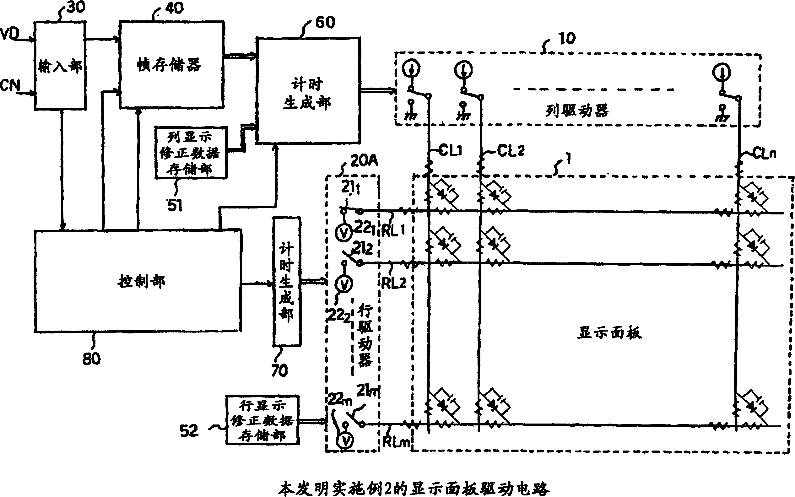
[0043] figure 2 It is a configuration diagram showing a display panel driving circuit according to Embodiment 2 of the present invention. right with figure 1 The same elements are attached with the same symbols.

[0044] The display panel driving circuit is provided with a column display correction data storage unit 51 and a row display correction data storage unit 52 instead of figure 1 The pixels in the display correction data storage unit 50, and instead of the row driver 20, a row driver 20A having a different function is provided.

[0045] The column display correction data storage unit 51 stores correction data for performing brightness correction due to differences in resistance or capacitance of the column lines CLi. figure 1 The pixel display correction data storage unit 50 stores correction data for each pixel in one frame, but the column display correction data storage unit 51 only stores correction data for the number of column lines CL. In addition, since thi...


PUM


Abstract

The invention provides a display panel driving circuit capable of making display free of unevenness by correcting the nonuniformity of luminance due to a difference in the resistance etc., of a row line and column line of a display panel and to provide a driving method. Such correction data to attain the same luminance by increasing or decreasing the driving time for light emitting elements varying in the luminance on the basis of the light emitting element EL outputting the average luminance when the image data of the same luminance level is given is set, and is previously stored in a pixel display correction data storage section 50. The actual image data for the one line component stored in a frame memory 40 and the corresponding correction data for the one line component stored in the pixel display correction data storage section 50 are read out and are added by each pixel in a timing generation section 60 and the on-off of each driving switch 12 of a column driver 10 is controlled with the pulse width modulation signal by the result of the addition as a control signal.

Description

technical field [0001] The invention relates to a display panel drive circuit and a drive method for driving display panels such as liquid crystal displays or organic EL (Electronic Luminescence) panels. Background technique [0002] [Patent Document 1]: JP-A-2004-45702 [0003] The aforementioned Patent Document 1 proposes a liquid crystal display device whose purpose is to improve image reproducibility by compensating optical response characteristics while correcting grayscale characteristics of an input image signal based on color reproduction characteristics of a liquid crystal display panel. The liquid crystal display device has: a liquid crystal display panel for displaying an image, and a writing grayscale determination unit corresponding to a combination of grayscale transitions before and after one vertical period of an input image signal, A writing gradation level for the liquid crystal display panel is determined, and the writing gradation level determination uni...

Claims


Application Information

Patent Timeline
IPC IPC(8): G09G3/20
CPCG09G3/2014G09G2320/0233G09G2320/0285G09G3/3216G09G3/30G09G3/20
Inventor 木村直哉原哲郎绀藤晃清水隆之高柳治代福迫真一高山一郎
Owner OKI ELECTRIC IND CO LTD
Why Eureka
Try Eureka