Apparatus and method for high-speed transfer and centering of wafer substrates
What is Al technical title?
Al technical title is built by PatSnap Al team. It summarizes the technical point description of the patent document.
a technology of high-speed transfer and centering, applied in the field of electromechanical systems, can solve the problems of unsatisfactory centering solution of conventional wafer handling approaches
Inactive Publication Date: 2000-09-12
BROOKS AUTOMATION INC
View PDF11 Cites 118 Cited by
Summary
Abstract
Description
Claims
Application Information
AI Technical Summary
This helps you quickly interpret patents by identifying the three key elements:
Problems solved by technology
Method used
Benefits of technology
FIG. 6 is an electrical block diagram of control e
Problems solved by technology
Conventional wafer handling approaches, however,
Method used
Image
Click on the blue label to locate the original text in one second.
Reading with bidirectional positioning of images and text.
Examples
Embodiment Construction
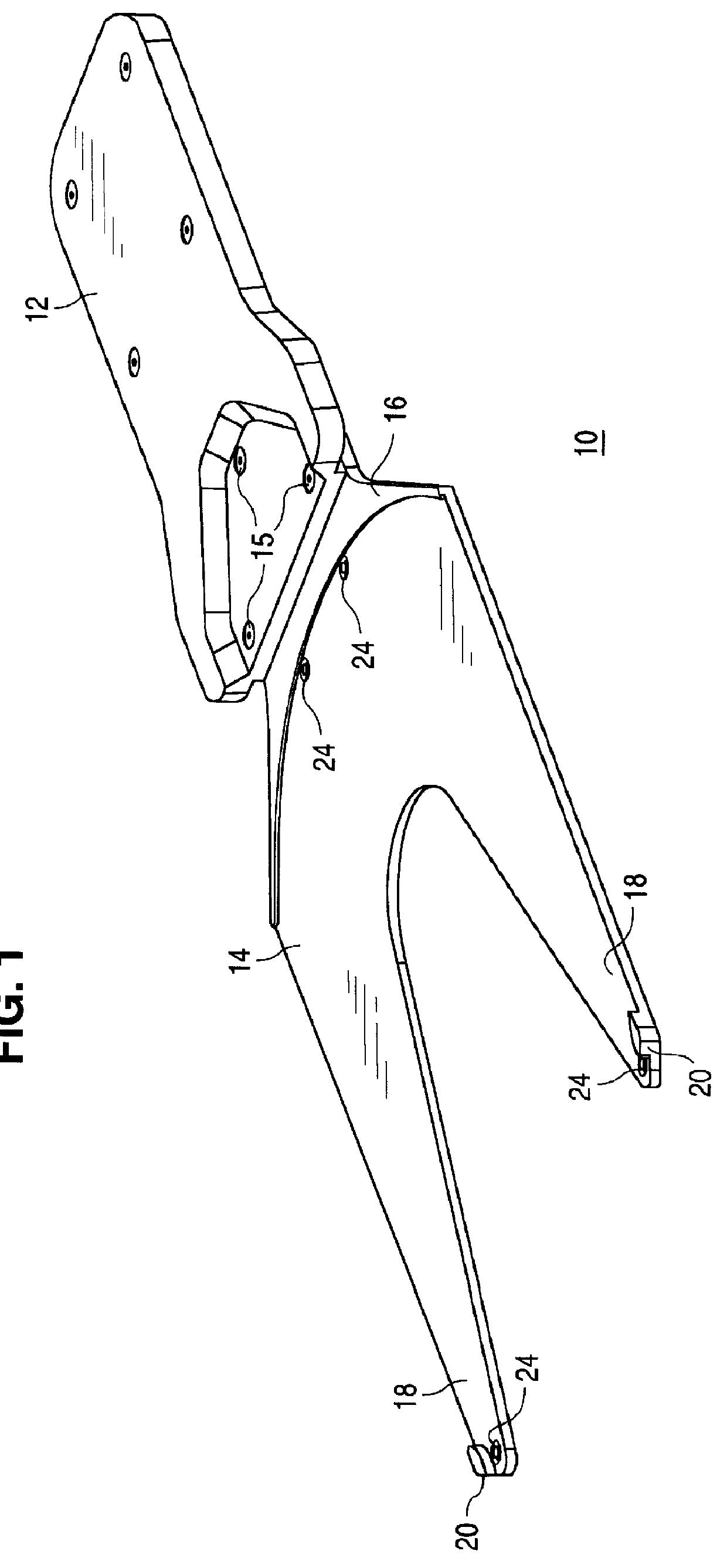
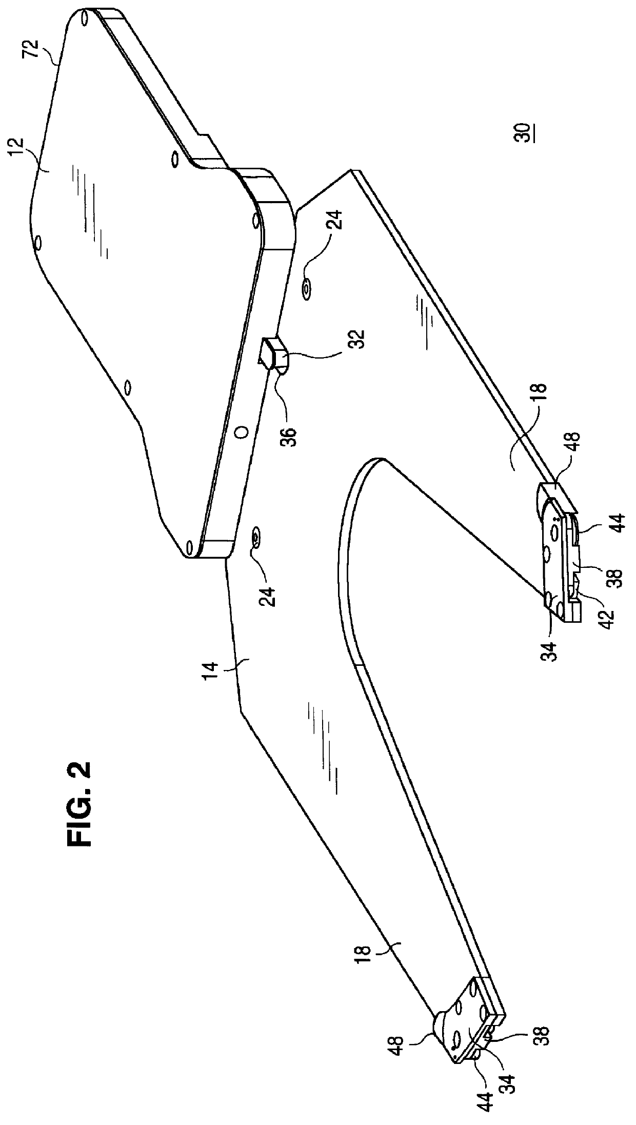
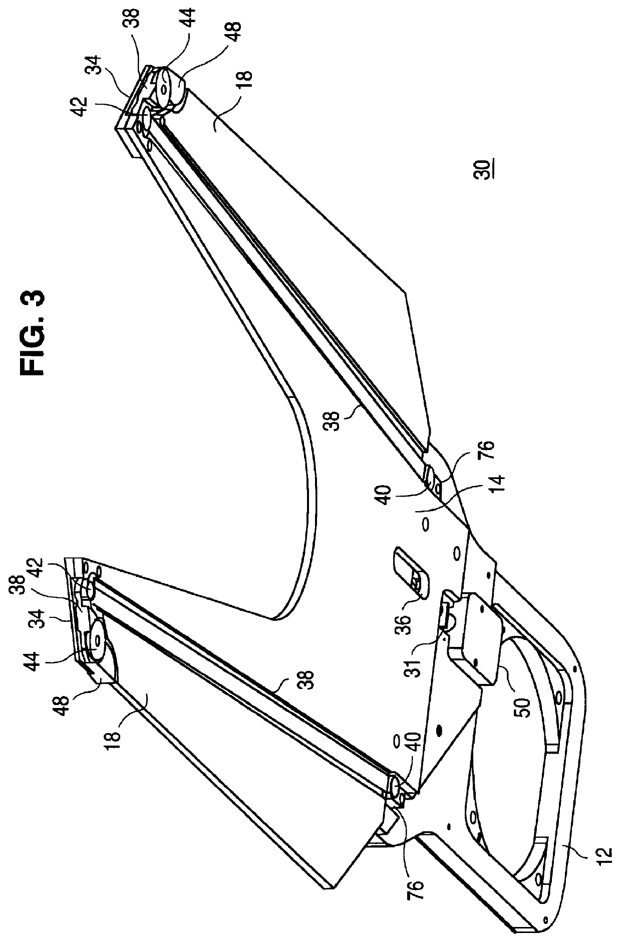
A preferred embodiment of the present invention is provided in a passive or active electromechanical apparatus or end effector and associated methodology for handling semiconductor wafers or similarly shaped substrates, flat objects or thin panels, particularly for centering wafers substantially on movable platform or robotic arm end effector having multiple alignment contacts. As described herein, contacts may be actuated by a solenoid, which effectively senses a wafer presence and position, as well as other diagnostic data. Also, as specified and claimed herein, the term "wafer" term is interpreted broadly, referring to any substantially flat or thin object or substrate.
Preferably, inventive apparatus contacts wafer about outer ring or wafer edge to reduce possible damage. The centering function is substantially accomplished without performing a true positional centering of a subject wafer relative to a robotic arm or end effector, as long as the subject wafer is physically aligne...
PUM
Abstract
An apparatus for centering and gripping semiconductor wafers. A solenoid is used to actuate two or three curved contacts. Power to the solenoid, and position information from the solenoid is transmitted along a pair of wires. To center the wafer, the solenoid is actuated and the contacts move radially towards the center of the wafer. The contacts grip the edge of the wafer and a pulse-width-modulation signal is used to determine solenoid position as a function of back electromotive force value or waveform. During handling, the contacts hold the wafer such that the wafer does not move relative to the apparatus.
Description
The invention relates to an electromechanical equipment for robotically moving semiconductor substrates, and particularly to wafer transfer and centering techniques.BACKGROUND OF INVENTIONDuring semiconductor manufacturing or processing, silicon wafers are moved between processing equipment, typically using robotic techniques. Because wafers are fragile and increasingly larger in size, careful handling and positioning is desirable. In particular, during a transfer, efficient wafer centering on a transfer platform is important. Conventional wafer handling approaches, however, do not provide satisfactory centering solution. For example, see U.S. Pat. Nos. 5,556,147, 5,570,994, 5,636,964, 5,647,626, 5,664,931.SUMMARY OF INVENTIONThe invention resides in an electromechanical system for centering a semiconductor wafer substantially on a movable platform having multiple alignment contacts. Preferably, contacts are actuated by a solenoid, which senses a wafer presence and position, as well...
Claims
Application Information
Patent Timeline
Application Date:The date an application was filed.
Publication Date:The date a patent or application was officially published.
First Publication Date:The earliest publication date of a patent with the same application number.
Issue Date:Publication date of the patent grant document.
PCT Entry Date:The Entry date of PCT National Phase.
Estimated Expiry Date:The statutory expiry date of a patent right according to the Patent Law, and it is the longest term of protection that the patent right can achieve without the termination of the patent right due to other reasons(Term extension factor has been taken into account ).
Invalid Date:Actual expiry date is based on effective date or publication date of legal transaction data of invalid patent.
IPC IPC(8): H01L21/67H01L21/687H01L21/68
CPCH01L21/68H01L21/68707Y10S414/141
Inventor THOMAS, DONALD JEFFREYAALUND, MARTIN PETERROY, ROBERTRISI, MICHAEL