Thin film transistor array substrate and fabricating method thereof

A technology of thin film transistors and array substrates, which is applied in the field of display panels and its manufacturing, and can solve problems such as light leakage in peripheral circuit areas

Inactive Publication Date: 2006-04-26
CHUNGHWA PICTURE TUBES LTD
View PDF0 Cites 21 Cited by
  • Summary
  • Abstract
  • Description
  • Claims
  • Application Information

AI Technical Summary

Problems solved by technology

[0007] In view of this, the object of the present invention is to provide a thin film transistor array substrate and its manufacturing method to solve the problem of light leakage caused by the peripheral circuit area

Method used


Image

  • Thin film transistor array substrate and fabricating method thereof
  • Thin film transistor array substrate and fabricating method thereof
  • Thin film transistor array substrate and fabricating method thereof

Examples


Embodiment Construction

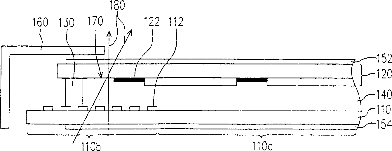
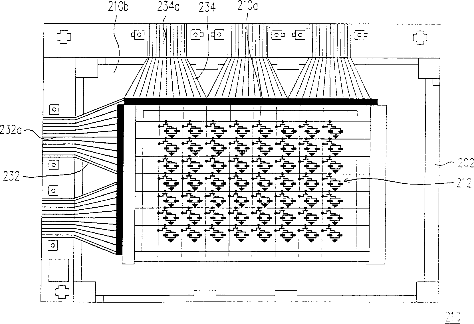
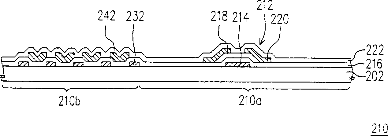
[0047] Please refer to figure 2 and 3 , figure 2 and 3 They are respectively a top view schematic diagram and a partial cross-sectional schematic diagram of a thin film transistor array substrate of the present invention. The thin film transistor array substrate 210 can be divided into, for example, a pixel area 210a and a peripheral line area 210b located on the periphery of the pixel area 210a, wherein the transparent substrate 202 in the pixel area 210a is provided with a thin film transistor array 212 composed of a plurality of thin film transistors and pixel electrodes. (not shown in the figure), and the transparent substrate 202 in the peripheral circuit area 210 b is provided with a plurality of leads connected to the thin film transistor array, which may be gate wiring 232 or source wiring 234 , for example. In addition, the ends of the gate wiring 232 and the source wiring 234 are respectively connected to a plurality of first pads 232 a and a plurality of second...


PUM


Abstract

The manufacture method for a TFT array base comprises: while manufacturing the TFT for pixel zone, forming light-screening layer between lead wires in round circuit by metal layer to shield zone easy leak light between source / drain layer or grid layer; besides, adding out stabilization voltage on light-screening layer to reduce signal disturbance of wires. Thereby, it can detect the TFT array and whether there is a short circuit between lead wire and light-screening layer by said out-added voltage simultaneously.

Description

technical field [0001] The present invention relates to a display panel and its manufacturing method, and in particular to a thin film transistor array substrate and its manufacturing method. Background technique [0002] With the substantial progress of computer performance and the high development of Internet and multimedia technology, the transmission of image information has mostly changed from analog to digital transmission. In order to adapt to the modern life style, the volume of video or image devices is becoming thinner and thinner day by day. The traditional cathode ray tube (Cathode Ray Tube, CRT) display has been monopolizing the display market in recent years because of its excellent display quality and economy. However, for the environment where individuals operate multiple terminals / display devices on the table, or from the perspective of environmental protection, if the trend of energy saving is predicted, there are still many problems in the space utilizati...

Claims


Application Information

Patent Timeline
Patent Type & Authority Applications(China)
IPC IPC(8): H01L27/02G02F1/136H01L21/77
Inventor 许汉东刘文雄何建国
Owner CHUNGHWA PICTURE TUBES LTD
Why Eureka
Try Eureka