
Light-conducting panel and production thereof

A manufacturing method and light guide plate technology, applied in manufacturing tools, optics, nonlinear optics, etc., can solve the problems of not meeting high-volume production, difficulty in modifying the mold core, time-consuming processing, etc., to improve light reflection and refraction effects, The effect of high yield of manufacturing process and improvement of light uniformity

Inactive Publication Date: 2006-05-31
NANO PRECISION
View PDF0 Cites 5 Cited by
  • Summary
  • Abstract
  • Description
  • Claims
  • Application Information

AI Technical Summary

Problems solved by technology

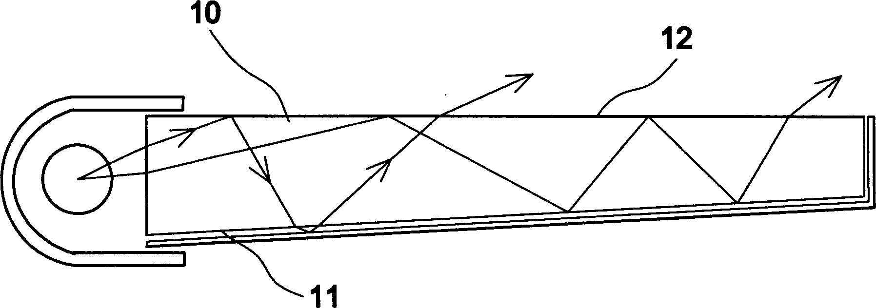
[0003] see figure 1 As shown, the conventional light guide plate 10 uses the principle of total reflection to transmit the light provided by the light source to the far end of the light guide plate 10, and then uses the dots 13 on the bottom surface 11 of the light guide plate to destroy the total reflection, so as to guide the light to the front of the light guide plate 12. The traditional manufacturing method of the light guide plate is to print the designed pattern directly on the light guide plate to form dots. Because the printing dot particles are not fine enough and the viscosity of the ink is not easy to control, the light uniformity and quality uniformity will be poor. It is not easy to control, and it is not a one-time molding, so the processing is time-consuming, and it does not meet the needs of high-volume production; another manufacturing method is disclosed in Taiwan, China Patent No. 514766, which first coats a photoresist on a flat substrate After exposing and developing the photoresist, a copper seed layer is planted, and then a nickel mold core is formed on the surface of the copper seed crystal by electroforming, and then the mold core is separated from the flat substrate, and then The copper seed crystal is etched away to form a nickel core, and finally the light guide plate of a backlight module is formed by injection molding of the core. However, many manufacturing processes (such as coating, exposure, etc.) , electroforming, etc.), and the modification of the mold core is not easy; therefore, the above-mentioned methods cannot achieve high-volume production, simplify the manufacturing process, and produce light guide plates with better optical effects.

Method used


Image

  • Light-conducting panel and production thereof
  • Light-conducting panel and production thereof
  • Light-conducting panel and production thereof

Examples


Embodiment Construction

[0029] Relevant present invention is for achieving the above-mentioned purpose, the technical means that adopts and all the other effects, hereby give a preferred embodiment, and cooperate drawing to illustrate as follows:

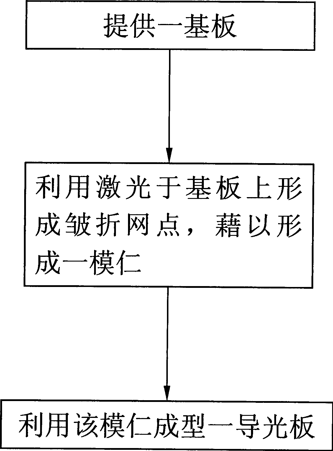
[0030] see figure 2 As shown, the manufacturing method of the light guide plate includes the steps: (A) providing a substrate 21; (B) using at least one laser to irradiate different positions on the substrate 21 to form a wrinkle dot 22 at each position, In order to form a mold core 20; and (C) utilize the mold core 20 to form a light guide plate 30 (such as Figure 5 shown).

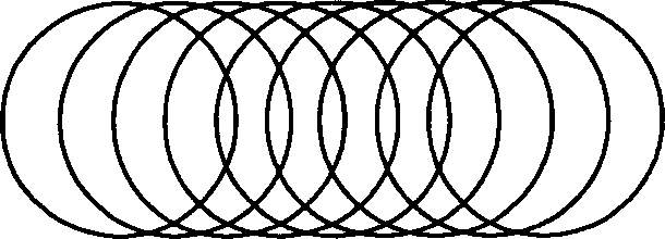
[0031] Its detailed steps, at first, provide a substrate 21 of metal or acrylic material, then provide a laser beam above the substrate 21, and repeatedly irradiate the same position on the substrate 21 to form a wrinkle network point 22 (such as Figure 4 shown), and then move the laser beam or move the substrate, and use the laser beam to repeatedly irradiate the substrate 21 t...


PUM


Abstract

A light guide plate consists of a base plate with a surface set with multiple ripple lattice point for raising optical effect and light evenness of light guide plate. Its preparing method includes shining a laser on different position of base plate to form a ripple lattice point at each position for preparing a model and utilizing said model to form a light guide plate.

Description

[technical field] [0001] The invention relates to a backlight module, in particular to a light guide plate applied to the backlight module and a manufacturing method thereof. [Background technique] [0002] The light guide plate is one of the key components of the backlight module. However, with the market demand for high brightness, high output and low cost, in order to maintain the market competitiveness of the light guide plate, the manufacturing method of the light guide plate needs to be researched and developed by the relevant industry. . [0003] see figure 1 As shown, the conventional light guide plate 10 uses the principle of total reflection to transmit the light provided by the light source to the far end of the light guide plate 10, and then uses the dots 13 on the bottom surface 11 of the light guide plate to destroy the total reflection, so as to guide the light to the front of the light guide plate 12. The traditional manufacturing method of the light guide ...

Claims


Application Information

Patent Timeline
Patent Type & Authority Applications(China)
IPC IPC(8): G02B5/02B23K26/36G02F1/1335
Inventor 陈汉荣许建宏王瑞仁
Owner NANO PRECISION
Learn More