Liquid crystal display device, manufacturing method and electronic apparatus

A liquid crystal display device and display area technology, applied in transistors, static indicators, optics, etc., can solve problems such as poor display and decreased contrast display characteristics, and achieve the effect of improving display characteristics and reducing area

Active Publication Date: 2006-06-07
BOE TECH GRP CO LTD
View PDF1 Cites 5 Cited by
  • Summary
  • Abstract
  • Description
  • Claims
  • Application Information

AI Technical Summary

Problems solved by technology

Therefore, the following problem is reflected, that is, when the substrate surface is viewed from the vertical direction, there is a predetermined width on the stepped portion, and the region corresponding to the stepped portion becomes a display-defective region, resulting in a decrease in display characteristics such as contrast.

Method used


Image

  • Liquid crystal display device, manufacturing method and electronic apparatus
  • Liquid crystal display device, manufacturing method and electronic apparatus
  • Liquid crystal display device, manufacturing method and electronic apparatus

Examples


no. 1 Embodiment approach

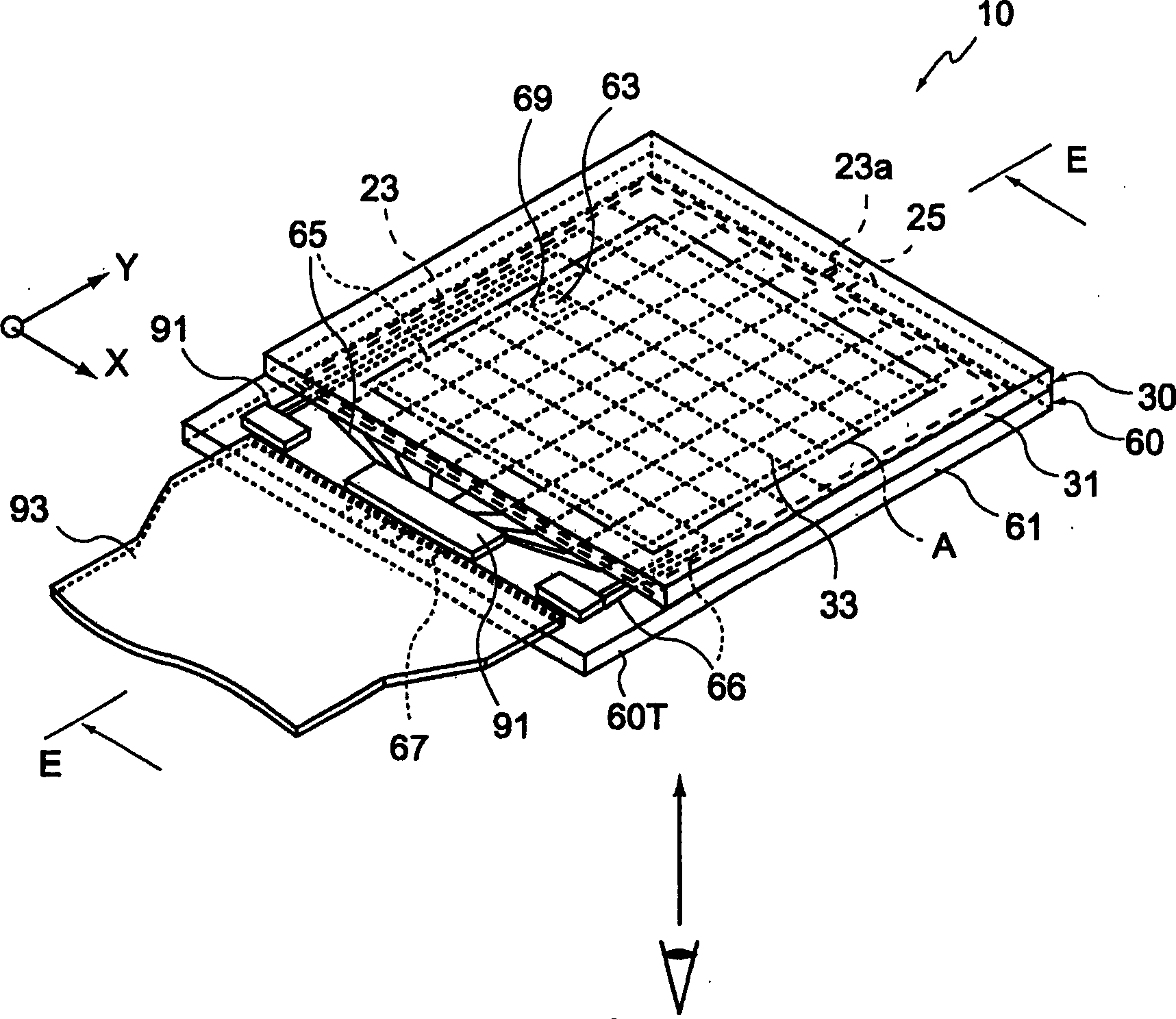
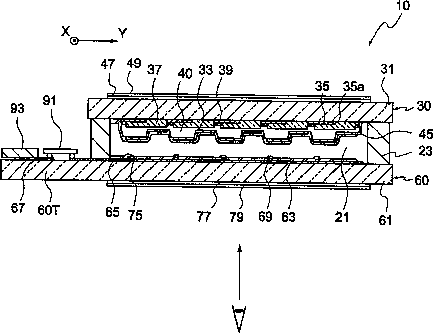
[0074] The first embodiment is a transflective liquid crystal display device comprising: a first substrate provided with a first electrode; a second substrate provided with a second electrode; and a liquid crystal material sandwiched between the first substrate and the second substrate. and a display area including a plurality of pixels, the plurality of pixels respectively have a reflective area and a transmissive area.

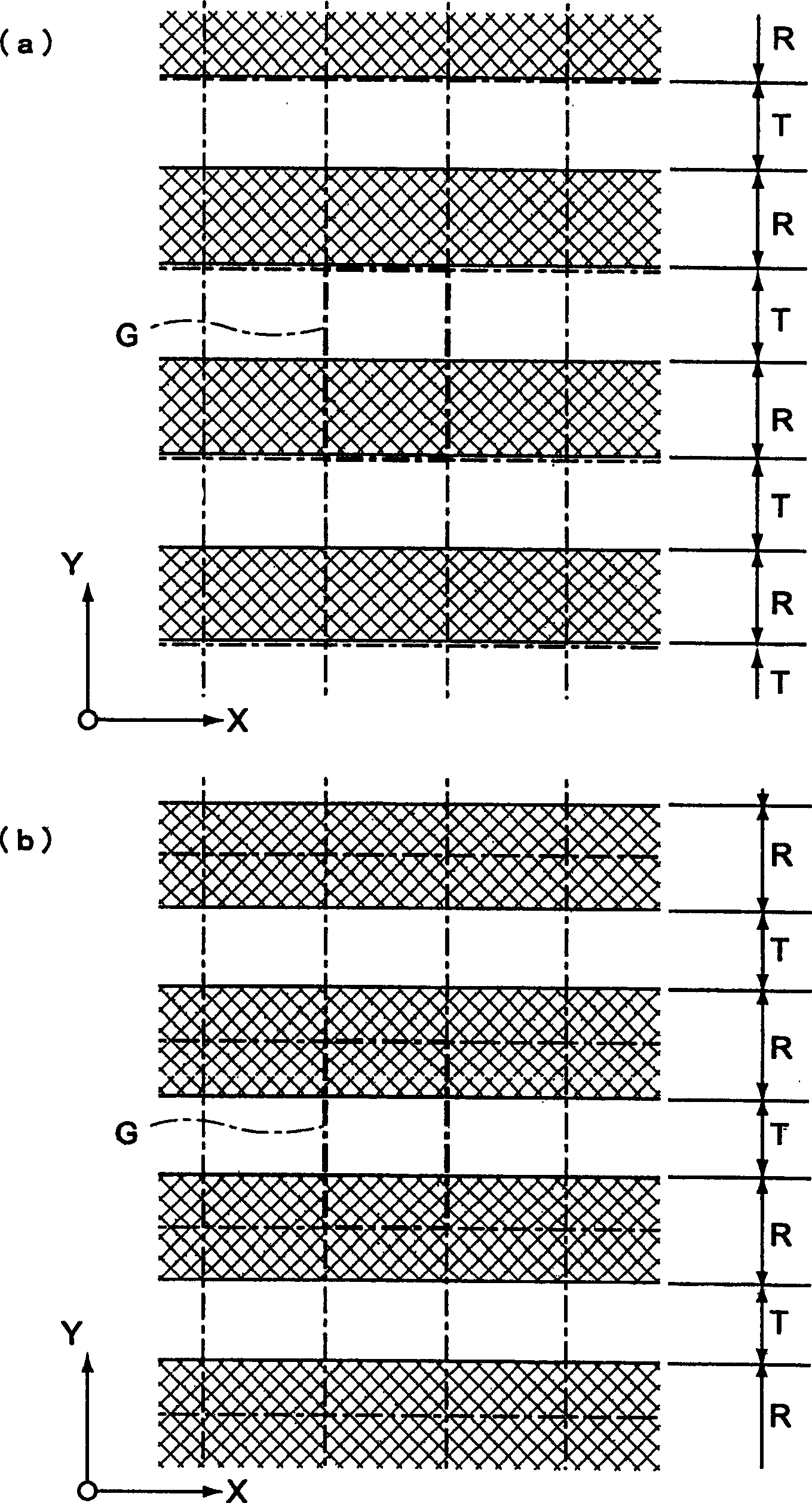
[0075] Furthermore, it is characterized in that the reflective region and the transmissive region are arranged in a strip shape across a pixel row formed by pixels arranged in one direction in the display region; An adjustment layer, the layer thickness adjustment layer has: a thick part arranged on the reflective region; and a thin part arranged on the transmissive region; The step part formed in the vertical direction, and has a relaxation part outside the display area, which is used to relax the step of the boundary between the thick layer part and the th...

no. 2 Embodiment approach

[0147] A second embodiment of the present invention is the method for manufacturing a liquid crystal display device according to the first embodiment, characterized by including:

[0148] A step of forming a photosensitive resin material layer on the first substrate;

[0149] In order to adjust the retardation in the reflective region and the transmissive region, a step of forming a layer thickness adjustment layer in which a thick part is arranged on the reflective region, a thin part is arranged on the transmissive region, and a thick layer is arranged in the display region The inclined surface of the boundary between the thick part and the thin part is formed along the vertical direction, and there is a relaxation part outside the display area, which is used to relax the step between the thick part and the thin part; and

[0150] The step of forming a first electrode on the upper layer of the layer thickness adjustment layer so that at least the first electrodes in the refl...

no. 3 Embodiment approach

[0194] A third embodiment is a transflective liquid crystal display device comprising: a first substrate provided with a first electrode; a second substrate provided with a second electrode; and a liquid crystal material sandwiched between the first substrate and the second electrode. between the substrates; and has a display area including a plurality of pixels, the plurality of pixels respectively have a reflective area and a transmissive area.

[0195] Furthermore, it is characterized in that the reflective region and the transmissive region are arranged in a strip shape across a pixel column formed by pixels arranged in one direction in the display region,

[0196] In order to adjust the retardation in the reflection area and the transmission area, the first substrate is provided with a layer thickness adjustment layer, and the layer thickness adjustment layer has: a thick layer portion arranged on the reflection area; and a thin layer portion arranged on the transmission a...


PUM


Abstract

PROBLEM TO BE SOLVED: To provide a liquid crystal display device which has less display defects due to a multi-gap step, a manufacturing method for a liquid crystal display device, and electronic equipment.

SOLUTION: A transflective type liquid crystal display device having a display region including a plurality of pixels having reflection region and transmission regions, is characterized in that: the reflection regions and transmission regions are arranged in stripes across pixel arrays of pixels arrayed in the display region in one direction; a 1st substrate has thick layer portions arranged in the reflection regions and thin layer portions arranged in the transmission regions, and also has step portions formed having oblique surfaces on borders between the thick layer portions and thin layer portions in the display region and layer thickness regulating layers having specified relaxation portions outside the display region; and 1st electrodes are formed on the layer thickness regulating layers and extended to outside the display regions respectively, and at least, 1st electrodes formed in reflection regions and transmission regions of the same pixel array are connected on relaxation portions.

COPYRIGHT: (C)2006,JPO&NCIPI

Description

technical field [0001] The present invention relates to a liquid crystal display device, its manufacturing method and electronic equipment. In particular, it relates to a liquid crystal display device, a method of manufacturing the liquid crystal display device, and an electronic device including the liquid crystal display device in which display defects due to multiple gap steps are reduced. Background technique [0002] Conventionally, a liquid crystal display device has been widely used as an image display device. In this liquid crystal display device, a pair of substrates on which electrodes are respectively formed are arranged to face each other, and the voltage applied to a plurality of pixels as the intersecting area of ​​each electrode is selectively The ground is turned on and off to modulate the light passing through the liquid crystal material in the pixel area to display images, characters, etc. [0003] As such a liquid crystal display device, there is a transf...

Claims


Application Information

Patent Timeline
Patent Type & Authority Applications(China)
IPC IPC(8): G02F1/136G02F1/133H01L29/786
CPCG02F1/133555G02F1/1343G02F2201/34G02F2203/02
Inventor 仓岛健
Owner BOE TECH GRP CO LTD
Why Eureka
Try Eureka