Method for drilling deep hole and PCB product obtained by same method

A new method and deep technology, which is applied in the direction of mechanically removing conductive materials, electrical components, printed circuits, etc., can solve problems such as poor depth drilling accuracy, and achieve the effect of improving depth accuracy and improving control accuracy

Inactive Publication Date: 2006-06-14
WUS PRINTED CIRCUIT (KUNSHAN) CO LTD
View PDF0 Cites 44 Cited by
  • Summary
  • Abstract
  • Description
  • Claims
  • Application Information

AI Technical Summary

Problems solved by technology

[0008] The technical problem to be solved by the present invention is to provide a new method of deep drilling that can effectively solve the problem of poor depth drilling accuracy caused by plate thickness uniformity, thereby improving the control accuracy of deep drilling, and by this method PCB finished products obtained by drilling

Method used


Image

  • Method for drilling deep hole and PCB product obtained by same method
  • Method for drilling deep hole and PCB product obtained by same method
  • Method for drilling deep hole and PCB product obtained by same method

Examples


Embodiment 1

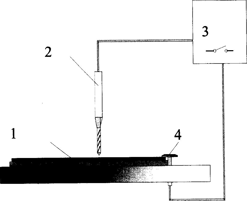
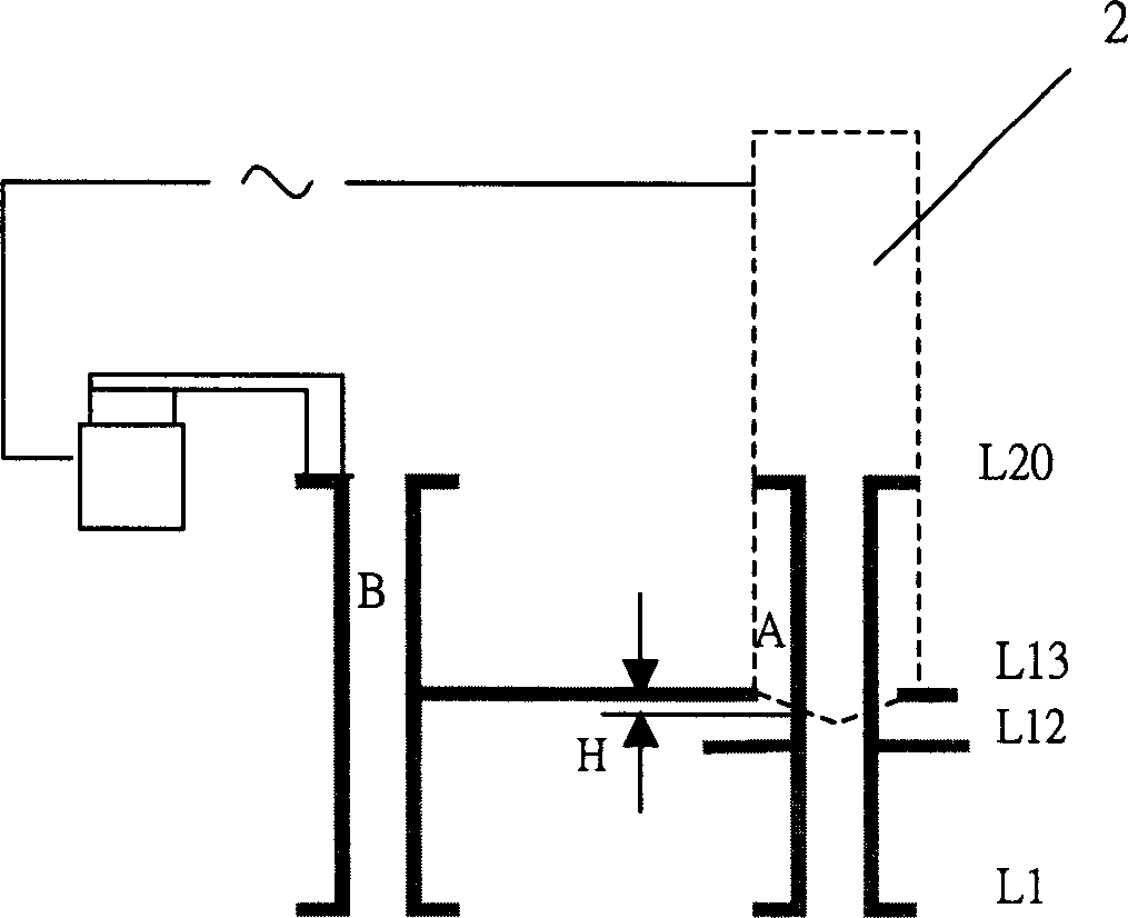
[0033] According to the customer's requirement to control the drilling depth between L12-L13, the present invention performs deep drilling operations on the production plate through the following methods:

[0034] like image 3 As shown, find the POWER layer closest to L12 between the L20-L13 layers (assuming that the POWER layer is the L13 layer), and set a via hole B on the outside of the board to connect with the POWER layer; increase the diameter of the drill needle 2 as shown in the figure Then start drilling, and when the drill is drilled down, it will be connected to the POWER layer (L13) for conduction, resulting in the formation of the machine control circuit; point A in the figure is regarded as the zero point, and the H value is regarded as the depth that needs to be controlled when drilling down. Doing so can avoid the impact of uneven plate thickness on depth control, and can greatly improve the control accuracy of drilling.

Embodiment 2

[0036] According to the customer's requirement to control the drilling depth between L12-L13, the present invention performs deep drilling operations through the following methods:

[0037] like Figure 4 As shown, some depth test holes Z1 are drilled on the upper surface of the production board, that is, the area requiring deep drilling on the aluminum cover plate 1, and depth test holes Z2 are drilled on the edge of the upper target layer L13, and depth test holes Z2 are drilled on the edge of the lower target layer. Drill depth test hole Z3 on the edge of the L12 board;

[0038] Add G87, G88, G89 and other functional commands to the machine control software, so that the machine can detect the depth values ​​of Z1 and Z2, and make a judgment on the drilling depth value based on the positions of Z1 and Z2;

[0039] G87, G88, and G89 are written in the program. When the G87 command is executed, the machine detects the position of the upper surface of the production board, whi...


PUM


Abstract

This invention discloses a new method for deep drilling and PCB products got from it, which sets the platform control loop on the POWER layer in the board and begins computing the designed depth from the place contacting the POWER by the drilling pin or drills the test holes of Z1,Z2 and Z3 on the necessary drilled regions of the upper surface, the upper target layer and the lower target layer then adds G87, G88 and G89 functional instructions on the control software of the platform to detect the depth values of Z1 and Z2 and judges the drilled depth value based on their positions, finally the platform adds a compensation value of a drill point to the depth of (Z2+Z3)/2 to drill.

Description

technical field [0001] The invention belongs to the technical field of printed circuit board (PCB) manufacturing, and relates to a new method for deep drilling and a finished PCB product obtained by drilling through the method. Background technique [0002] The so-called PCB depth drilling means drilling a through hole into a hole consisting of a part of the through hole and a part of the non-through hole by mechanical drilling. The depth of the non-through hole is usually controlled between two adjacent inner layers. And the depth accuracy is required to be controlled at ±1mil (thousandth of an inch) (such as figure 1 Shown, among them: L1...Ln represents which layer). [0003] The existing PCB deep drilling method is to use the chuck conductive feedback system, that is, to use the existing deep drilling machine, add a conductive aluminum cover plate 1 on the surface of the production board, and the tail end of the drill needle 2 passes through the conductive switch. 3. T...

Claims


Application Information

Patent Timeline
Patent Type & Authority Applications(China)
IPC IPC(8): H05K3/04H05K1/00
Inventor 徐国成
Owner WUS PRINTED CIRCUIT (KUNSHAN) CO LTD
Why Eureka
Try Eureka