Thin film transistor panel and liquid crystal display using the same

A technology of thin film transistors and liquid crystal display devices, which can be used in transistors, static indicators, instruments, etc., and can solve problems such as limiting power supply capacity

Active Publication Date: 2006-06-21
SAMSUNG DISPLAY CO LTD
View PDF0 Cites 45 Cited by
  • Summary
  • Abstract
  • Description
  • Claims
  • Application Information

AI Technical Summary

Problems solved by technology

[0006] Batteries used as power sources in mobile technologies such as cellular phones have limited power capacity

Method used


Image

  • Thin film transistor panel and liquid crystal display using the same
  • Thin film transistor panel and liquid crystal display using the same
  • Thin film transistor panel and liquid crystal display using the same

Examples


Embodiment Construction

[0060] Preferred embodiments of the present invention will be described more fully below with reference to the accompanying drawings. However, this invention may be embodied in different forms and should not be construed as limited to the embodiments set forth herein.

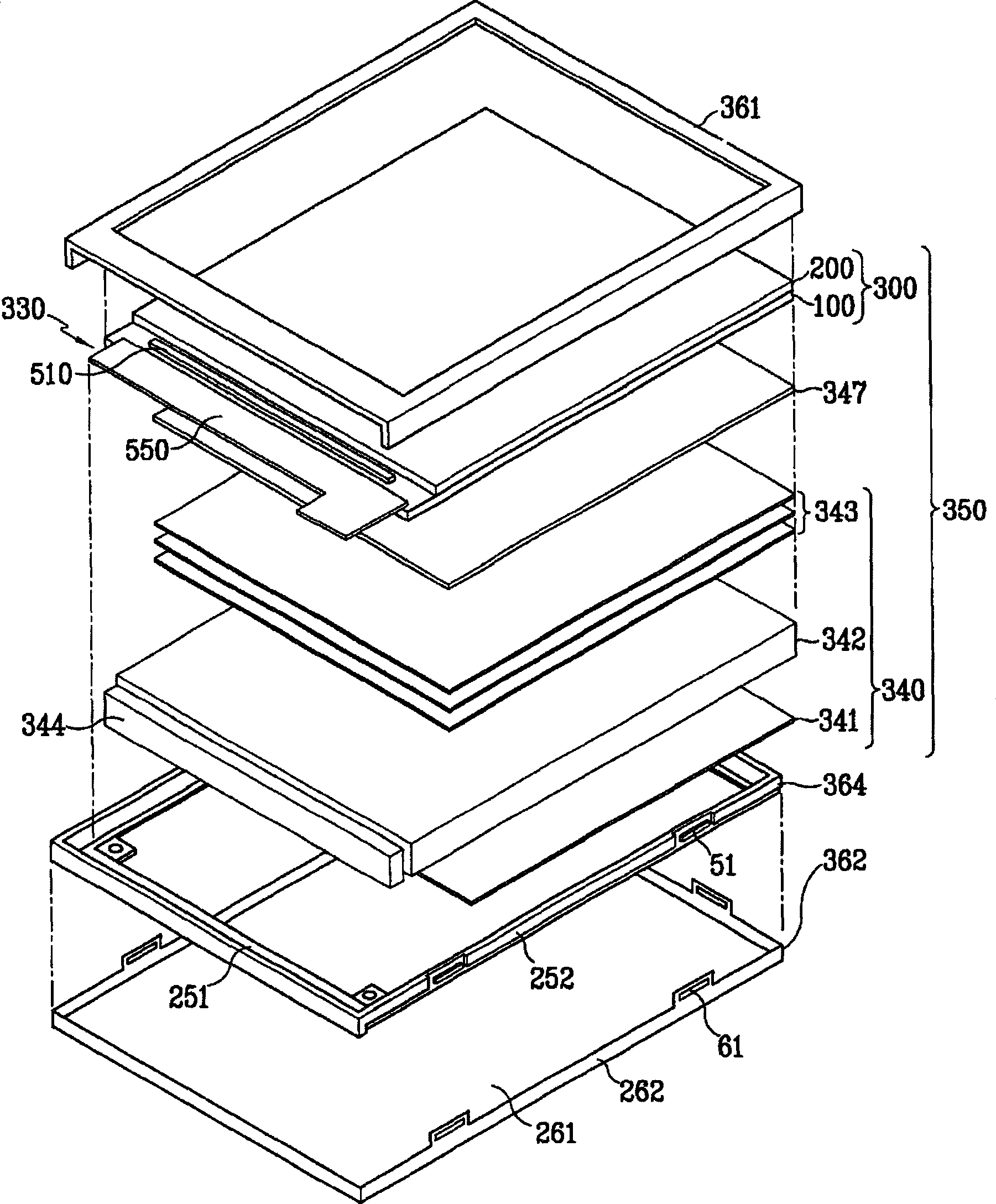
[0061] figure 1 is an exploded perspective view schematically showing an LCD according to an embodiment of the present invention.

[0062] refer to figure 1 , the LCD according to an embodiment of the present invention includes: an LC panel assembly 330 for displaying an image using light; a backlight assembly 340 for generating light; a selective reflection film 347 disposed between the LC panel assembly 330 and the backlight assembly 340 the molding frame 364 for accommodating the LC panel assembly 330, the selective reflection film 347, and the backlight assembly 340 therein; the upper bracket 361 and the lower bracket 362 to surround and support the above-mentioned elements.

[0063] The LC panel assembl...


PUM


Abstract

The invention discloses an LCD device, which comprises: a transmissive LCD panel assembly; a backlight assembly for providing light to the LCD panel assembly; a selective reflection film arranged between the backlight assembly and the LCD panel assembly. A display area of ​​the LCD has a low-resolution area and a high-resolution area, and pixels formed in the low-resolution area are larger than pixels formed in the high-resolution area.

Description

technical field [0001] The present invention relates to a liquid crystal display (LCD) and a thin film transistor (TFT) panel for the liquid crystal display. Background technique [0002] Generally, an LCD includes a pair of panels respectively having electrodes on inner surfaces thereof and a dielectrically anisotropic liquid crystal layer interposed between the panels. In the LCD, the change of the voltage difference between the field generation electrodes, that is, the change of the electric field intensity generated by the electrodes, changes the transmittance of light passing through the liquid crystal layer, thereby obtaining the desired image by controlling the voltage difference between the electrodes . [0003] In an LCD, the light may be natural light or artificial light emitted from a light source employed by the LCD. [0004] A backlight is a representative device for providing artificial light in an LCD, for example, the backlight utili...

Claims


Application Information

Patent Timeline
Patent Type & Authority Applications(China)
IPC IPC(8): G02F1/136G02F1/133G02F1/1335H01L29/786
CPCG02F1/13306G02F1/133555G02F1/136286
Inventor 鱼基汉金炯杰金尚佑李承珪安宝煐朴源祥金宰贤尹海荣李宰瑛埃尔纳·博达勒娃车圣恩张映珠林载翊郑基勋
Owner SAMSUNG DISPLAY CO LTD
Why Eureka
Try Eureka