Method and apparatus for improved MOS gating to reduce miller capacitance and switching losses

A switch and electrode technology, applied in the field of metal oxide semiconductor field effect transistors, can solve the problem of reducing the channel width and achieve the effect of less switching time and switching loss

Inactive Publication Date: 2006-07-26
FAIRCHILD SEMICON CORP
View PDF0 Cites 21 Cited by
  • Summary
  • Abstract
  • Description
  • Claims
  • Application Information

AI Technical Summary

Problems solved by technology

However, the ability to further reduce the channel width is limited by the ability to etch the narrow channel, and there is a corresponding need to be able to fill this narrow channel with gate electrode material

Method used


Image

  • Method and apparatus for improved MOS gating to reduce miller capacitance and switching losses
  • Method and apparatus for improved MOS gating to reduce miller capacitance and switching losses
  • Method and apparatus for improved MOS gating to reduce miller capacitance and switching losses

Examples


Embodiment Construction

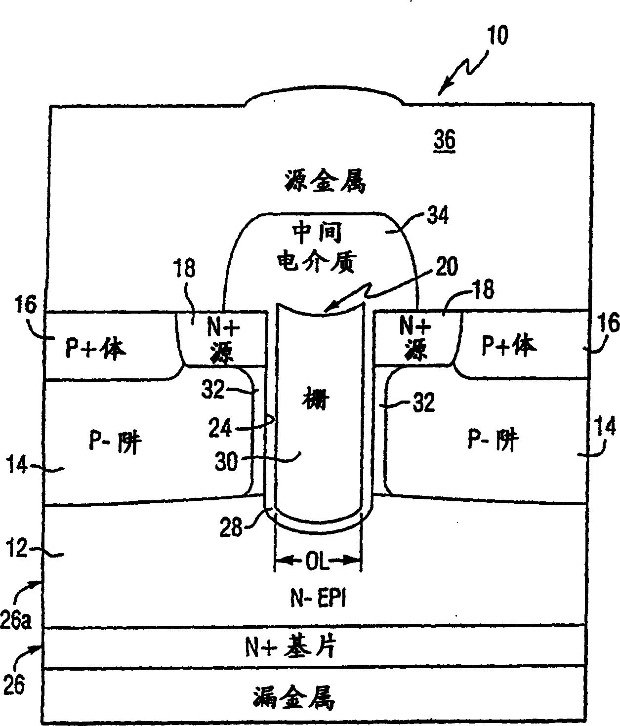
[0025] Referring now to the accompanying drawings in particular figure 1 , which shows a schematic cross-sectional view of a prior art trench-gated MOSFET device. MOSFET device 10 includes drain region 12 , well region 14 , body region 16 , source region 18 , gate region 20 and channel 24 , all of which are formed on substrate 26 .

[0026] More specifically, the N+ type substrate 26 includes an upper layer 26a in which the N- drain region 12 is formed. The P-type well region 14 is located above the drain region 12 . A heavily doped P+ body region 16 is defined within an upper surface (not indicated) of upper layer 26 a and a portion of well region 14 . A heavily doped N+ source region 18 is formed on the upper surface of upper layer 26 a and within a portion of well region 14 and adjacent to channel 24 . The sidewalls and bottom (not shown) of trench 24 are lined with a dielectric material 28, such as oxide. Gate region 20 is formed of conductive material 30, such as dope...


PUM


Abstract

A semiconductor gate structure includes a shielding electrode and a switching electrode. Portions of a shield electrode are located over the drain region and the well region. The first dielectric layer is located between the shielding electrode and the drain and well regions. Portions of switch electrodes are located over the well region and the source region. A second dielectric layer is located between the switch electrode and the well and source regions. A third dielectric layer is located between the shield electrode and the switch electrode.

Description

[0001] Related patent application reference [0002] This patent application claims the benefit of priority to US Provisional Patent Application Serial No. 60 / 405,369, filed August 23,2002. technical field [0003] This invention relates to semiconductors, and more particularly to metal oxide semiconductor field effect transistors (MOSFETs). Background technique [0004] MOSFETs are widely used in the field of switching, for example, switching power supplies hardly use other types of transistors. MOSFETs are suitable for this switching application because they have a relatively high switching speed and require low power. However, dynamic losses in MOSFETs account for a large percentage of the total losses in a DC-DC converter. The dynamic loss is directly proportional to the rise and fall time of the device, and the rise and fall time of the device is proportional to the gate-drain capacitance of the device, that is, the Miller capacitance (C GD or Q GD ) proportional to...

Claims


Application Information

Patent Timeline
Patent Type & Authority Applications(China)
IPC IPC(8): H01L29/76
CPCH01L29/407H01L29/7813H01L29/41H01L29/42376
Inventor 克里斯托弗·B.·库肯艾伦·艾本海威
Owner FAIRCHILD SEMICON CORP
Why Eureka
Try Eureka