Improvements to resonant line drivers

A driver circuit and circuit output technology, which is applied in transmission line coupling devices, transmission systems, logic circuits, etc., can solve problems such as signal interference

Inactive Publication Date: 2006-08-02
MIDAS GREEN
View PDF1 Cites 8 Cited by
  • Summary
  • Abstract
  • Description
  • Claims
  • Application Information

AI Technical Summary

Problems solved by technology

) Therefore, a signal that is input to the aforementioned IC and that is primarily coupled to VSSB due to its specific physical routing may suffer from severe interference when received by the receiver circuit in this IC

Method used


Image

  • Improvements to resonant line drivers
  • Improvements to resonant line drivers
  • Improvements to resonant line drivers

Examples


Embodiment Construction

[0056] go to Figure 8 , which displays the same Figure 6 A similar circuit as in , but instead of providing the reservoir capacitor entirely between the VSSD and VHHD circuit nodes, the reservoir capacitor is split into two capacitors, CR1 and CR2. CR1 provides capacitance between VSSD and VHHD, and CR2 provides capacitance between VDDD and VHHD. Because each of CR1 and CR2 provides a parallel charging capacitor, each of CR1 and CR2 can be made Figure 6 Half the value of CR in order to provide the same actual charge capacitance. But by utilizing split charging capacitors, making Figure 8 The driver 19 in is more symmetrical, so when a voltage change in the driver output signal VDO causes current to flow into or out of the interconnect 14, the return current flows back into the driver 19, which is equally divided between the package lead inductances LPL1 and LPL2.

[0057] Figure 9 show relative to Figure 8 The waveform generated by the circuit. Will Figure 7 and ...


PUM


Abstract

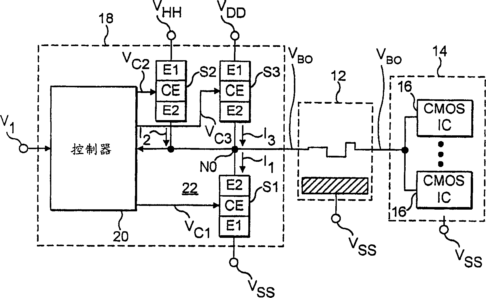
The present invention provides an electronic driver circuit for communicating a logic value along a conductor (12) from one part of a system (10) to another (14) by representing each of two logic values by one of two logic levels (VDD, VSS). A capacitor (CR1) reduces ground and power reference differences between a chip containing the driver and the board on which it is mounted. The capacitor also provides power and ground decoupling. According to another aspect, a controlled slew rate ramp initiates an incident or outbound wave or turn-on and circuits are described for this. The time taken to complete the controlled slew rate ramp can be adjusted. The arrangements allow reduced power consumption, whilst at the same time producing desirable signal characteristics.

Description

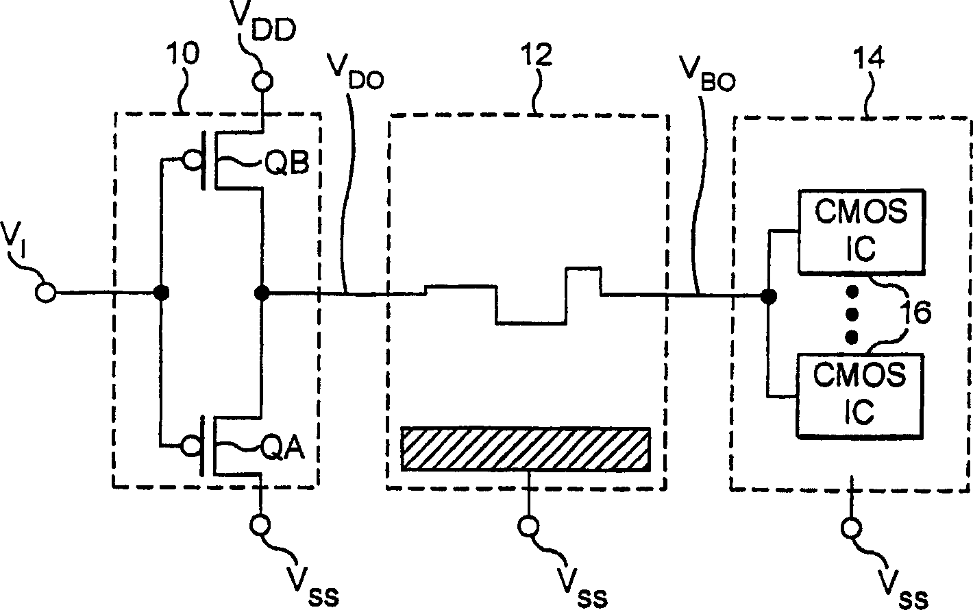
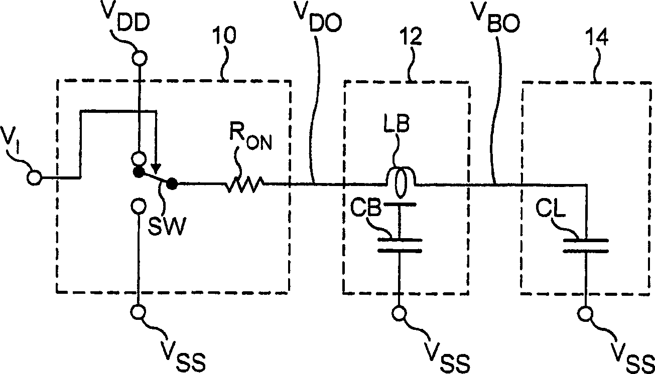
technical field [0001] The present invention relates to electronic circuits. More particularly, the present invention relates to improving the performance of electronic driver circuits of the type whose operation is to reduce power consumption. The present invention is concerned with achieving low power consumption in such driver circuits while producing desired signal characteristics. Background technique [0002] For many years, there have been conventional driver circuits that communicate logic values ​​from one part of a system to another by representing each of two logic values ​​at one of two voltage levels, respectively. For example, Figure Ia shows a conventional CMOS inverting driver 10 formed as part of an IC. In response to driver input voltage signal VI, output driver 10 generates an inverting driver voltage VDO. The driver 10 is connected to a load circuit 14 via electrical conductors 12 printed wiring board (PWD). Specifically, the electrical conductors 12 ...

Claims


Application Information

Patent Timeline
Patent Type & Authority Applications(China)
IPC IPC(8): H03K17/687H03K19/00H04L25/02
CPCH04L25/028H03K19/0019H04L25/0272
Inventor 杰弗里·P·哈维
Owner MIDAS GREEN
Why Eureka
Try Eureka