Exposure method and apparatus

An exposure method and technology of an exposure device, which are applied to the exposure device of a photoengraving process, an exposure method of a radiation-sensitive mask, a microlithography exposure device, etc., can solve the problem of increased hardening shrinkage, excessive irradiation energy, and inability to completely remove the Protective layer and other problems to achieve good plating effect

Inactive Publication Date: 2006-08-23
FUJIFILM CORP
View PDF2 Cites 2 Cited by
  • Summary
  • Abstract
  • Description
  • Claims
  • Application Information

AI Technical Summary

Problems solved by technology

[0010] However, if the irradiation energy is too large, the protective layer may not be completely removed after etching.
In addition, in the case of a solder resist film, if the irradiation energy is too large, the curing shrinkage increases due to excessive photopolymerization. As a result, the solder resist film may be damaged in the process of curing the solder resist film. The whole is easy to peel off

Method used


Image

  • Exposure method and apparatus
  • Exposure method and apparatus
  • Exposure method and apparatus

Examples


Embodiment Construction

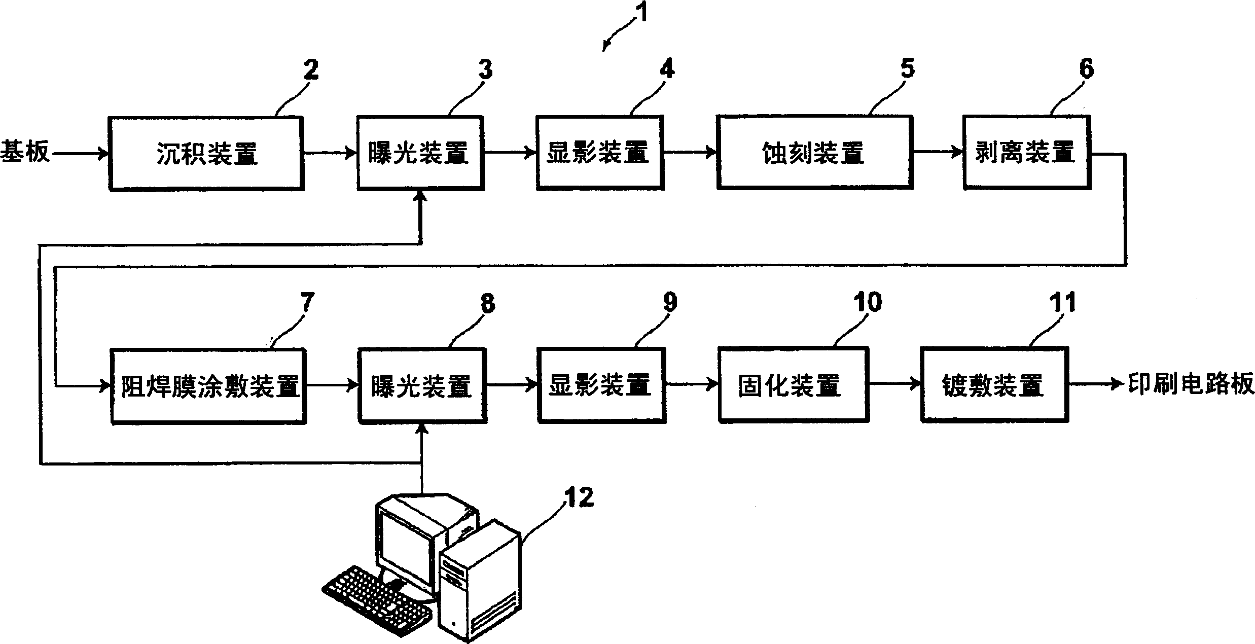
[0065] Embodiments of the present invention will be described below with reference to the drawings. figure 1 It is a schematic block diagram showing the configuration of a printed circuit board manufacturing system including an exposure apparatus according to an embodiment of the present invention. like figure 1 As shown, the printed circuit board manufacturing system 1 of this embodiment is equipped with: a lamination device 2, which laminates a photosensitive adhesive film (DFR) on a substrate formed of copper foil to form a protective layer; an exposure device 3, which exposes Matching display pattern; developing device 4, which develops the exposed protective layer to form a protective pattern with the same shape as the wiring pattern; etching device 5, which etches the copper foil on the substrate on which the protective pattern is formed to form a wiring pattern Stripping device 6, which peels off the protective layer remaining on the substrate after etching; Solder res...


PUM

PropertyMeasurementUnit
reflectanceaaaaaaaaaa
transmittivityaaaaaaaaaa

Abstract

When exposing a pattern on a recording medium, such as a printed wiring board on which a photosensitive layer having sensitivity to light, such as a resist layer or the like, is stacked, the photosensitive layer is prevented from unduly becoming irremovable or liable to be peeled off, while maintaining the adhesion of the layer. In order to achieve this, when a wiring pattern is exposed on a resist layer formed on a substrate by an exposure apparatus 3, irradiation energy of the exposure light is controlled to become greater in an edge portion of the wiring pattern than in the other portion of the wiring pattern.

Description

technical field [0001] The present invention relates to an exposure method and apparatus for exposing a predetermined pattern such as a wiring pattern of a printed circuit board on a photosensitive layer laminated on a recording medium such as a printed circuit board by using a light beam emitted from a laser light source. Background technique [0002] Various exposure apparatuses have been proposed in the past that perform image exposure with a light beam modulated according to image data using a spatial light modulation element such as a digital micromirror device (DMD). As one of the uses of such an exposure apparatus, it is known that it can be utilized in the manufacturing process of a printed wiring board (for example, refer patent document 1). [0003] In general, the following methods are used to manufacture printed circuit boards. First, on the conductive layer (such as copper thin film) formed on the substrate on which the wiring pattern is formed, a photosensitiv...

Claims


Application Information

Patent Timeline
Patent Type & Authority Applications(China)
IPC IPC(8): G03F7/20H01L21/027H05K3/00
CPCG03F1/144H05K3/0082G03F7/2022G03F7/70425H05K3/064G03F7/20H05K3/00G03F1/00
Inventor 佐佐木义晴
Owner FUJIFILM CORP
Why Eureka
Try Eureka