

Printed circuit board inspecting method and apparatus inspection logic setting method and apparatus
A substrate inspection and setting method technology, which is applied to measuring devices, optical devices, image data processing, etc., can solve the problems of difficult substrate inspection, high device cost, and large capacity, and achieve simple and high-speed processing and suppression The effect of usage
- Summary
- Abstract
- Description
- Claims
- Application Information
AI Technical Summary
Problems solved by technology
Method used
Image

Examples
no. 1 approach
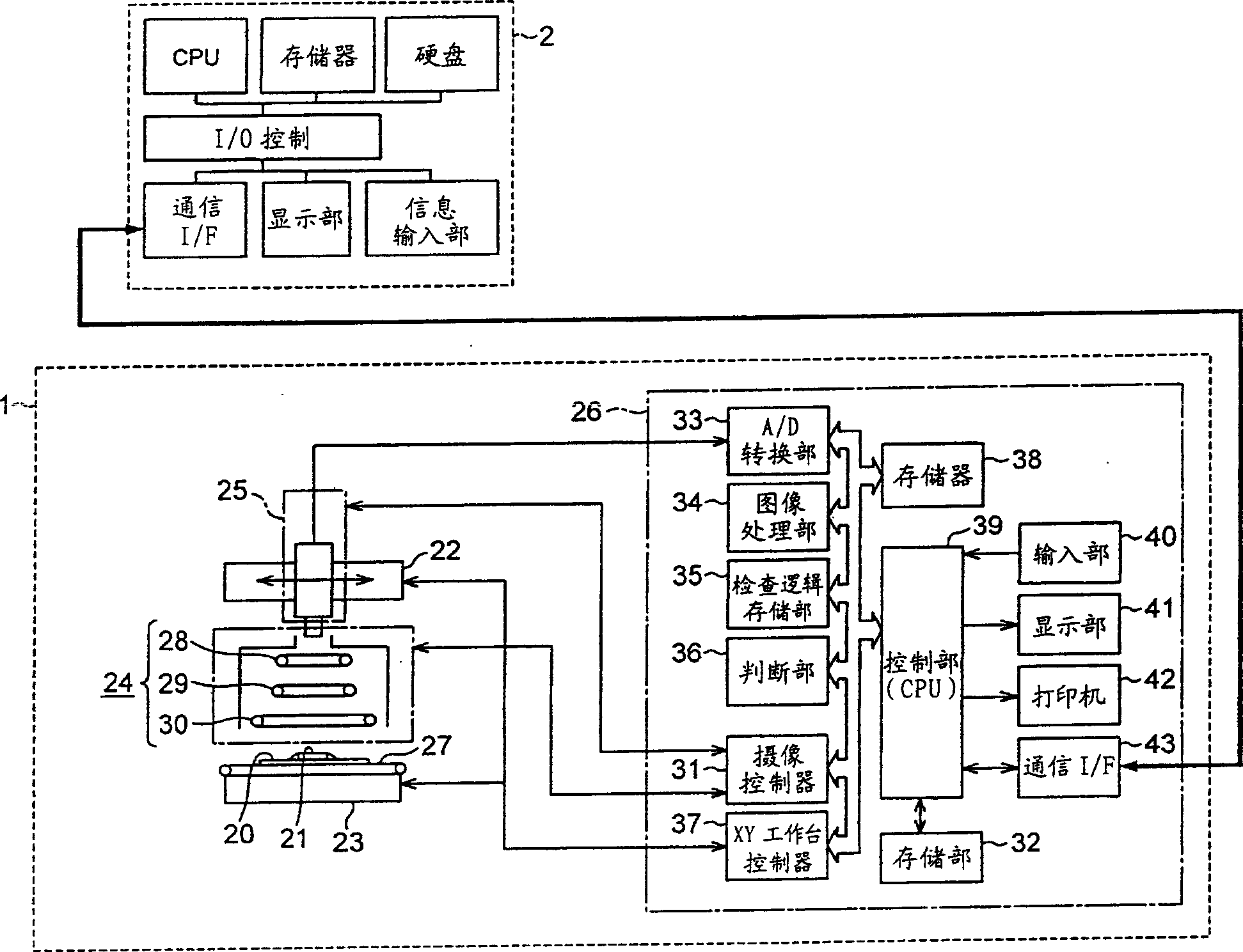
[0068] (Structure of board inspection system)
[0069] figure 1 The hardware configuration of the substrate inspection system according to the embodiment of the present invention is shown.
[0070] The substrate inspection system includes a substrate inspection device 1 that executes substrate inspection processing, and an inspection logic setting device 2 that automatically generates inspection logic used in the substrate inspection process of the substrate inspection device 1 . The substrate inspection device 1 and the inspection logic setting device 2 can be performed via a wired or wireless network, or a recording medium such as MO or DVD. image or transfer of electronic data such as parameters. In addition, in the present embodiment, the substrate inspection device 1 and the inspection logic setting device 2 are separate structures, but the substrate inspection device body may incorporate the function of the inspection logic setting device to form an integrated structu...
no. 2 approach
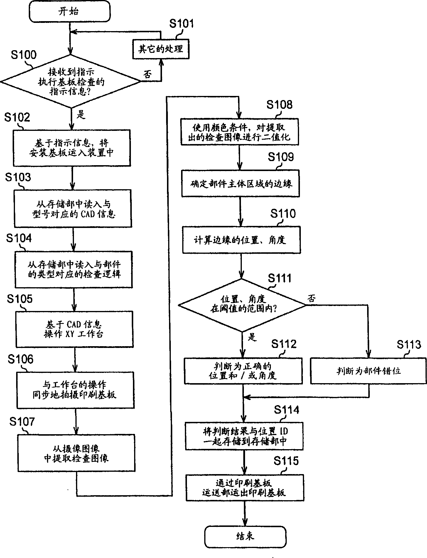
[0137] In the above-described first embodiment, the misalignment of the IC-based component is inspected focusing on the edge of the component main body portion. However, depending on the type of part, there may be deviation or unevenness in the color distribution of the main part of the part, making it difficult to determine the edge. For example, when characters or symbols are printed on the surface of the component body, or when the surface of the component body is deformed by heating during reflow, etc., color unevenness of the component body may occur. Therefore, in the second embodiment of the present invention, focusing on the fact that a plurality of leads are arranged linearly along the edge in IC components, the straight line connecting the plurality of leads (hereinafter referred to as " The position and angle of the lead alignment line"), thereby checking for component misalignment.
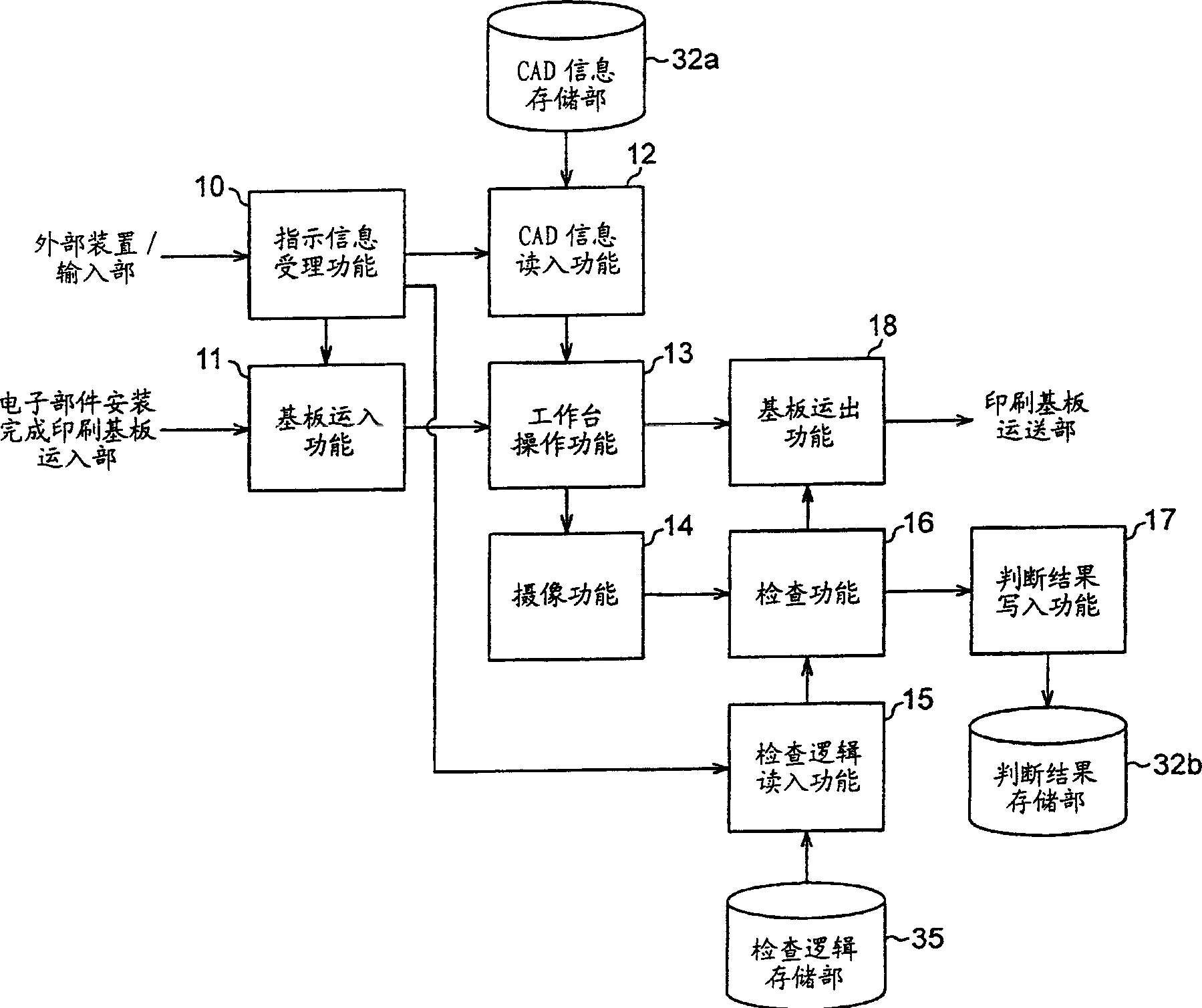
[0138] (Substrate inspection processing)
[0139] First, refer to Figure 12 Th...
PUM
 Abstract
Description
Claims
Application Information