Semiconductor storage system and method for transmission of write and read data

A storage system and data reading technology, which is applied in the direction of digital memory information, information storage, static memory, etc., can solve the problem of difficult DQS signal synchronization, reduce the number of pins, simplify symbol synchronization, and reduce the number of lines Effect

Inactive Publication Date: 2006-08-30
INFINEON TECH AG
View PDF0 Cites 0 Cited by
  • Summary
  • Abstract
  • Description
  • Claims
  • Application Information

AI Technical Summary

Problems solved by technology

Synchronization bursts interfere with data communication on the bus due to possible conflicts with read or write data, and the transmission of discrete DQS signals for synchronization is always difficult if the data transfer rate is high

Method used


Image

  • Semiconductor storage system and method for transmission of write and read data
  • Semiconductor storage system and method for transmission of write and read data
  • Semiconductor storage system and method for transmission of write and read data

Examples


Embodiment Construction

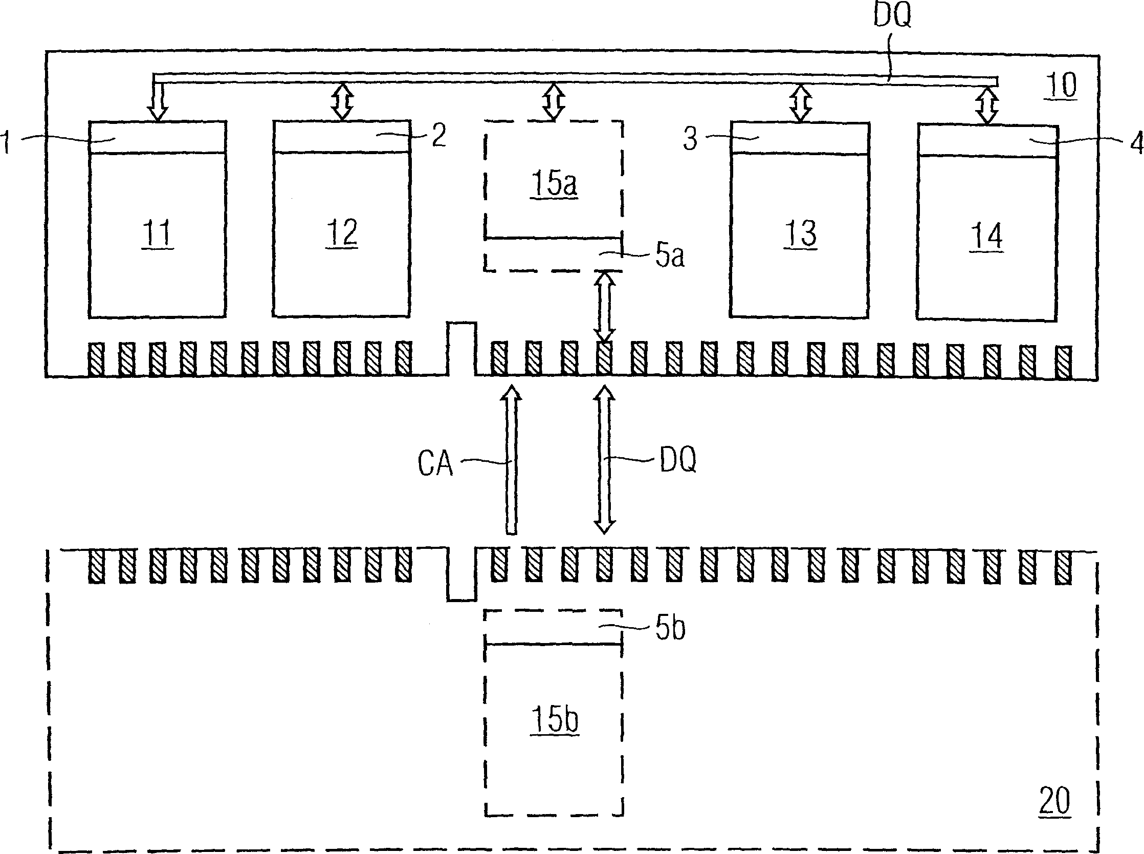
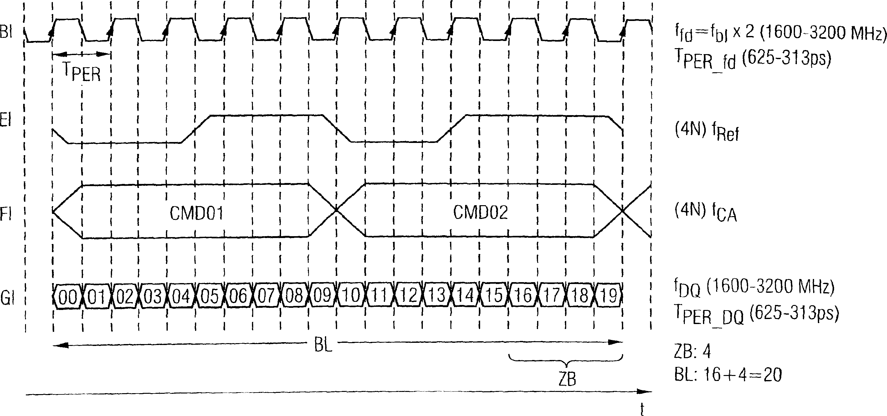
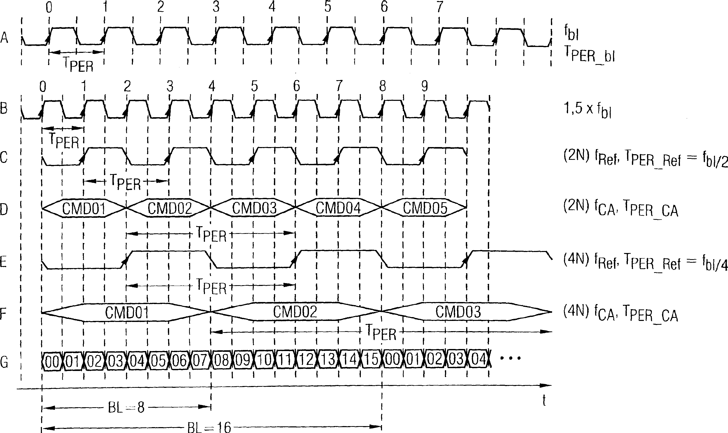
[0020] pass below figure 1 with figure 2 The description of the preferred embodiment of the invention is preceded by a description of the prior art signal-time diagram of FIG. 3 illustrating a conventional method for transmitting write and read data signals. According to this transmission method and based on the frequency f shown in the first line A b1 base clock, for example with a period length of 1250-625ps at P PR_b1 Corresponding frequency range f b1 = within 800-1600MHz, and based on the frequency 1.5xf shown in the second line B and derived directly from the base clock according to line A b1 A basic clock, for example in the frequency range 1333-2400MHz corresponding to a period length of 750-416ps, is generated according to the "2N" rule either having a period length T shown in the third line C per_ref The reference clock f ref , the "2N" rule means that the CA unit interval is twice the period length of the base clock according to the second line B. Alternative...


PUM


Abstract

The invention relates to a semi-conductor memory for transmitting written or read data signal between interface circuits, which comprises at least one memory device, memory controller and selective register, wherein each data signal is transmitted at the signal pulse sequence with special pulse sequence length. And the invention is characterized in that: several additional bits expanding the pulse sequence are transmitted with each n signal pulse.

Description

technical field [0001] The present invention relates to a semiconductor storage system. More particularly, the present invention relates to a semiconductor memory system having at least one memory device, a memory controller unit and optionally a register unit. Each of these elements includes an interface circuit, and the invention also relates to a method of transmitting write and read data signals between the interface circuits, the data signals being transmitted in signal bursts having a specific burst length . Background technique [0002] Now, a discrete ECC module capable of detecting and possibly correcting a channel error or a data error generated by a DRAM error is provided in a memory module mounted with a high-speed semiconductor memory device for detecting or correcting errors. However, traditional DIMM memory modules commonly used in desktop personal computers do not have the ability to detect and correct errors. Additional modules for detecting and / or correc...

Claims


Application Information

Patent Timeline
Patent Type & Authority Applications(China)
IPC IPC(8): G11C7/00
CPCG11C5/04G11C7/1018
Inventor H·鲁克鲍尔C·西歇尔特D·萨维纳克P·格雷戈里乌斯P·瓦尔纳
Owner INFINEON TECH AG
Why Eureka
Try Eureka