Dual-voltage three-state buffer circuit

A three-state buffer, dual-voltage technology, applied in the direction of logic circuit, logic circuit connection/interface layout, logic circuit coupling/interface using field effect transistors, etc., can solve the excessive instability of inverter ratio and increase energy consumption Circuit layout area and other issues

Active Publication Date: 2006-08-30
TAIWAN SEMICON MFG CO LTD
View PDF0 Cites 9 Cited by
  • Summary
  • Abstract
  • Description
  • Claims
  • Application Information

AI Technical Summary

Problems solved by technology

[0007] Although buffer 100 reduces post-driver crossover current and uses two-level shifters 102 and 104 to convert low-level voltages to high-level voltages, due to timing issues, the inverters driving post-driver transistors 112 and 114 Ratio is too unstable
In addition, level shifters 102 and 104 and inverters 156 and 158 increase power consumption and circuit layout area

Method used


Image

  • Dual-voltage three-state buffer circuit
  • Dual-voltage three-state buffer circuit
  • Dual-voltage three-state buffer circuit

Examples


Embodiment Construction

[0034] In order to make the above objects, features and advantages of the present invention more comprehensible, a preferred embodiment will be described in detail below together with the accompanying drawings.

[0035] The present invention proposes a dual-voltage tri-state buffer circuit with a tri-state level shifter, which can simplify circuit design. As such, the present invention reduces circuit layout area and reduces power consumption through dual voltage circuits.

[0036] The present invention will improve the design of dual voltage tri-state buffers.

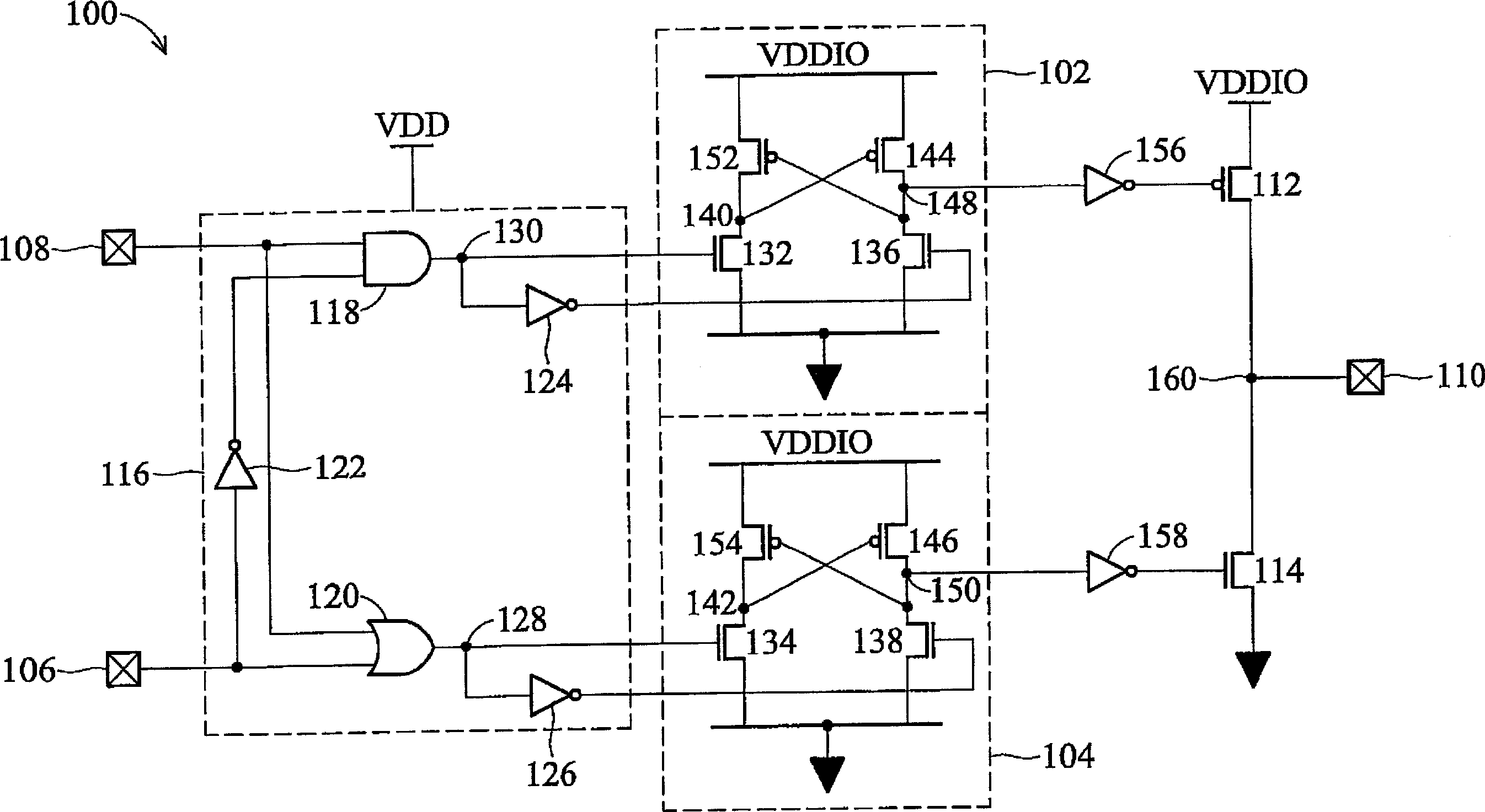
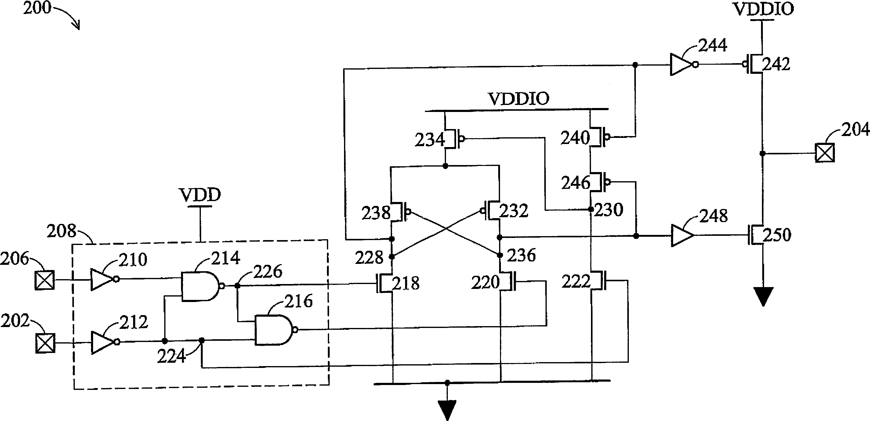
[0037] Figure 2A is a dual-voltage tri-state buffer circuit 200 according to the first embodiment of the present invention. Circuit 200 includes a level shifter and pull-up and pull-down switches.

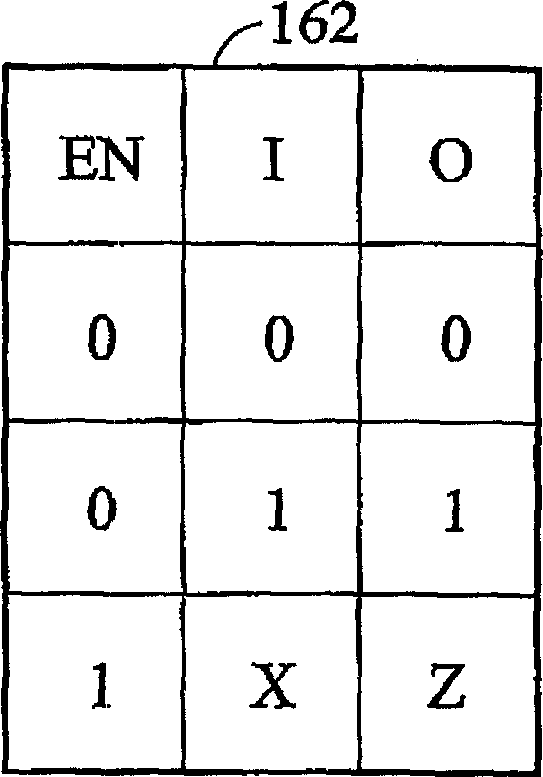
[0038] Like buffer 100, circuit 200 also switches between three different states and has two modes of operation: normal mode and tri-state mode. The normal mode occurs when the enable pin 202 is set to a low level, an...


PUM


Abstract

A dual-voltage three-state buffer circuit controls a post driver circuit to operate in a three-state mode and includes a tri-state logic control module operated under a low supply voltage, a level shifter for receiving one or more inputs from the tri-state logic control module and operating with an output control circuit for controlling two differential outputs of the level shifter, and a post driver circuit driven by the two differential outputs of the level shifter, wherein the level shifter, the output control circuit, an the post driver circuit are operated under a high supply voltage, and wherein when the tri-state logic control module generates the inputs for putting the post driver circuit in a high impedance state, the output control circuit operates with the level shifter to turn off the PMOS and NMOS transistors of the post driver circuit while isolating the level shifter from a high supply voltage.

Description

technical field [0001] The present invention relates to an integrated circuit, and in particular to an improved design of a dual-voltage tri-state buffer circuit using a tri-state level shifter. Background technique [0002] The existing dual-voltage tri-state buffer includes a two-level shifter for controlling a post driver circuit, and it is composed of PMOS and NMOS transistors. The two-level shifter converts lower voltage signals into higher voltage signals. The post-driver circuit determines the output of the entire circuit by deciding which transistors are on or off. However, since PMOS transistors are driven more slowly than NMOS transistors, the time required to turn on or off PMOS and NMOS transistors is different. Since different input signals may establish different paths for signal transmission, and some paths may take more time, therefore, the time required for each level shifter to output signals is also different. According to these timing differences, in t...

Claims


Application Information

Patent Timeline
Patent Type & Authority Applications(China)
IPC IPC(8): H03K19/0185
CPCH03K19/0013H03K19/09429H03K19/0016
Inventor 陈国基陈克明
Owner TAIWAN SEMICON MFG CO LTD
Why Eureka
Try Eureka