Conductive ball, method of forming electrode of electronic part, electronic part and electronic equipment

A technology of electronic components and electronic equipment, applied in semiconductor/solid-state device components, welding equipment, electrical components, etc., can solve problems such as poor reliability, easy disconnection, and weak mechanical strength of the connection, so as to prevent cracks and Disconnection, prevent bad effect

Active Publication Date: 2006-08-30
SEKISUI CHEM CO LTD
View PDF2 Cites 7 Cited by
  • Summary
  • Abstract
  • Description
  • Claims
  • Application Information

AI Technical Summary

Problems solved by technology

Due to this interface 17, there is a problem that sufficient conductivity cannot be obtained at the connection portion between the above-mentioned electronic component 5 and the circuit board 11.
In addition, due to the above-mentioned interface 17, there is also a problem that the mechanical strength of the connection part is very weak
Even when sufficient electrical conductivity can be obtained, since the mechanical strength of the connection portion forming the above-mentioned interface 17 is very weak, there is a problem that disconnection easily occurs and reliability is poor.

Method used


Image

  • Conductive ball, method of forming electrode of electronic part, electronic part and electronic equipment
  • Conductive ball, method of forming electrode of electronic part, electronic part and electronic equipment
  • Conductive ball, method of forming electrode of electronic part, electronic part and electronic equipment

Examples


no. 1 Embodiment

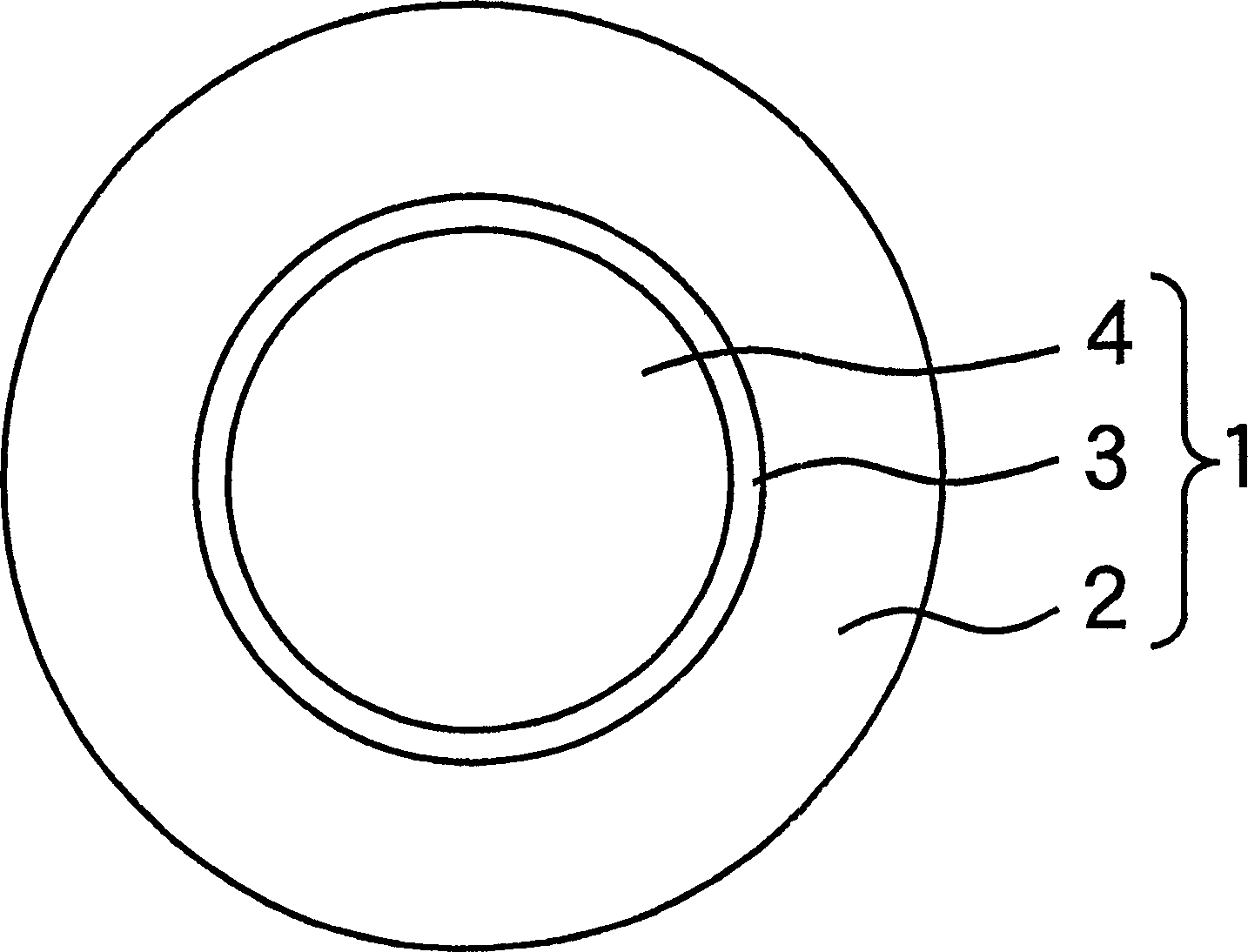
[0092] In this embodiment, an alloy of Sn-5.5Ag composition is used as the solder alloy layer 2 of the above-mentioned conductive ball member 1, and external electrodes are formed on the pads of the electronic component. An alloy layer obtained by sequentially performing Ni plating on Cu and flash Au plating was used on the pad.

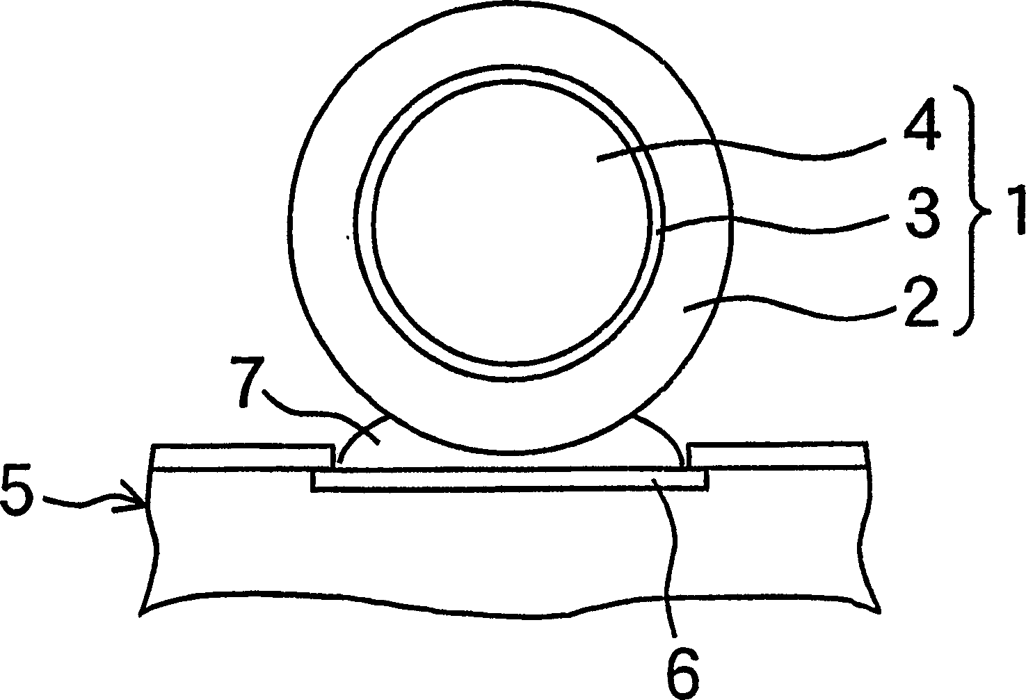
[0093] Figure 2A , B are diagrams showing steps of forming external electrodes on electronic components. exist Figure 2A In , the above-mentioned conductive ball member 1 is disposed on the pad 6 of the above-mentioned electronic component through the solder 7 . In order to remove the oxidized film on the surface of the solder alloy layer 2 or the surface of the pad 6 and maintain appropriate wettability of both, the above-mentioned flux 7 requires an appropriate degree of activity. However, since it becomes a cause of residue after the reflow process, corrosion of metal, etc., it needs to have appropriate removability. In this example, RMA typ...

no. 2 Embodiment

[0128] In this embodiment, a solder alloy having a composition of Sn-3.5Ag is used, and electrodes are formed using a flux different from that in the first embodiment. Since the process of forming electrodes is the same as that of Embodiment 1, detailed description thereof will be omitted. The difference from the first embodiment is that a high-halogen-containing (RA type) flux Deltalux 533 (manufactured by Senju Metal Industries) was used. The flux contains 0.22% Cl. In addition, 240 degreeC peak was used as the reflow temperature condition.

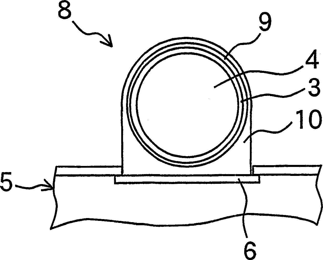
[0129] In the electrode of this example, no exposure of the SnCu layer was observed. This is because the content of the Cl element contained in the flux is increased from 0.04% in the first embodiment to 0.2%, which improves the activity of the flux. This improvement in flux activity can prevent the exposure of the SnCu layer, which is poor in adhesion, even with a solder alloy having a Sn-3.5Ag component. Therefore, even in the cas...


PUM

PropertyMeasurementUnit
liquidus temperatureaaaaaaaaaa

Abstract

Conductive ball part (1) is produced by applying a coating layer composed of Cu layer (3) and layer of Sn-5.5Ag alloy of noneutectic composition (2) onto approximately spherical core (4) constituted of a nonmetallic material. The conductive ball part (1) is arranged through a flux on a land of electronic part, and reflow thereof is carried out at heating temperature whose peak temperature reaches 250 to 260 DEG C. The Sn-5.5Ag alloy of noneutectic composition is conditioned into a state in which solid phase portions and liquid crystal portions coexist to thereby attain relative reduction of fluidity with the result that an SnCu layer formed on the surface of the Cu layer (3) is fixed on the land without exposure. An electrode can be formed without exposure of the SnCu layer of relatively poor solder wettability. Joint zone of excellent electrical conduction and mechanical strength can be formed between the electronic part and a circuit board.

Description

technical field [0001] The present invention relates to a conductive ball, a method for forming an electrode of an electronic component, an electronic component and an electronic device. Background technique [0002] In recent years, miniaturization and high density of electronic components have been pursued in response to demands for miniaturization and weight reduction of electronic equipment typified by mobile phones and portable information devices. Therefore, a bare-chip package structure in which an LSI (Large-Scale Integration) chip is directly mounted on a circuit board as an electronic component, or a so-called chip size package (Chip Size Package; hereinafter referred to as LSI chip) has been proposed in which the shape and size are as close as possible to an LSI chip. It is a packaging structure in which electronic components of CSP are packaged on a circuit substrate. In these packaging structures, in order to increase the packaging density, the structural featu...

Claims


Application Information

Patent Timeline
Patent Type & Authority Applications(China)
IPC IPC(8): H01B5/00H01L21/60H05K3/34B23K35/14B22F1/02B23K35/26C22C13/00H01L23/12
CPCH05K3/3463H05K2201/10234H05K3/3436H01L2224/11H01L2224/05567H01L2224/05573H01L2224/05655H01L24/05Y02P70/50H01L2924/00014
Inventor 住川雅人村山里奈小川将志松下清人
Owner SEKISUI CHEM CO LTD
Why Eureka
Try Eureka