Power diode and manufacturing method
A technology of power diodes and manufacturing methods, applied in semiconductor/solid-state device manufacturing, electrical components, circuits, etc., can solve problems such as low stability, unstable high-temperature diffusion, and difficult breakdown voltage control
- Summary
- Abstract
- Description
- Claims
- Application Information
AI Technical Summary
Problems solved by technology
Method used
Image
Examples
Embodiment Construction
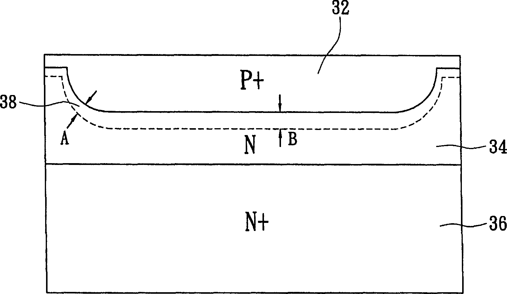
[0030] Please refer to image 3 , is a schematic diagram of the structure of the power diode of the present invention. The present invention includes: a first semiconductor layer 36 , a second semiconductor layer 34 and a third semiconductor layer 32 . Wherein the first semiconductor layer 36 is a semiconductor silicon substrate layer formed by the CZ / FZ / NTD method and is of the first conductivity type. The second semiconductor layer 34 is a semiconductor epitaxial layer, which is grown on the first semiconductor layer 36 by epitaxy, adjacent to the first semiconductor layer, and also has the first conductivity type, and the first conductivity The doping concentration of the type is smaller than the doping concentration of the first semiconductor layer. The third semiconductor layer 32 is a semiconductor diffusion layer, which is formed by second dopant diffusion with different depths, forms a P-N junction in the power diode, and forms a cylindrical curved surface junction ar...
PUM
 Abstract
Description
Claims
Application Information


