Alignment detection structure and alignment offset detection method

A technology for detecting structures and detection methods, which is applied in the direction of machine/structural component testing, measuring electricity, and measuring devices, and can solve problems such as complex detection methods, roughly estimated offsets, and misalignment offsets

Inactive Publication Date: 2006-10-11
AU OPTRONICS CORP
View PDF0 Cites 12 Cited by
  • Summary
  • Abstract
  • Description
  • Claims
  • Application Information

AI Technical Summary

Problems solved by technology

However, in the process of pressing, there will inevitably be mechanical or human errors, resulting in misalignment and deviation, so it is necessary to observe the deviation and re-adjust the machine
[0003] figure 1 It is a traditional method for detecting and evaluating the offset status of the glass substrate and chip bonding in the COG process. It uses a microscope to directly observe the position of the alignment mark on the opposite substrate after the chip is bonded in the COG process. Although the alignment mark on the chip The alignment mark 1 and the alignment mark 2 on the substrate have a fixed length and width between them, but if there is a deviation after the chip is pressed, because the two alignment marks are not completely sealed Therefore, when the offset occurs, we can only make a rough estimate to estimate the offset status, and cannot know the amount of offset clearly.
This method can only roughly estimate the possible offset direction and amount of the ma

Method used


Image

  • Alignment detection structure and alignment offset detection method
  • Alignment detection structure and alignment offset detection method
  • Alignment detection structure and alignment offset detection method

Examples


Embodiment Construction

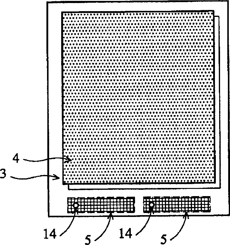
[0027] Please refer to the following figure 2 The alignment detection structure of a preferred embodiment of the present invention is described, which includes: a substrate 3 ; a color filter 4 ; and an alignment pattern 14 disposed in the die bonding area 5 on the substrate 3 . Since the following embodiments are described with the COG process, the substrate 3 is a glass substrate, but it should be noted that the present invention can also be applied to other lamination processes, such as plastic substrates.

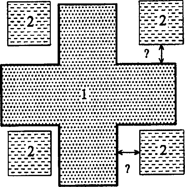
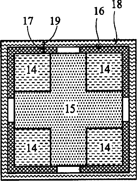
[0028] image 3 It is an enlarged view of the alignment detection structure of the present invention, wherein the alignment pattern 14 is completely complementary to the alignment mark 15 on the chip. In addition, the alignment pattern 14 has a first frame 16 with a known first width 17 located around the alignment pattern 14 . In this embodiment, the alignment marks 15 on the chip are cross-shaped, and the alignment patterns 14 are four square patterns located at fo...


PUM


Abstract

The invention relates to an aim detecting structure, which comprises an aim picture on the basic plate, and a frame with known width on the periphery of said picture. The invention can be used in COG (Chip-On-Glass) technique, that with the aim mark of chip, after COG pressing, judging the deflection amount via the relative position of aim mark and the frame; therefore, the invention can directly calculate the deflection after compressing chip to adjust the machine after COG process.

Description

technical field [0001] The present invention relates to an alignment detection structure and a detection method for alignment offset, and in particular to a substrate that can be used to detect chip pressing deviation after the chip is pressed in the COG (Chip-On-Glass) process. Alignment detection structure of displacement and method for detecting displacement thereof. Background technique [0002] Generally, the driving method of liquid crystal display is driven by the driver chip (IC), and some of the driver chips are pressed to the corresponding position on the substrate accurately through the high-temperature and high-pressure lamination process, so there will be The alignment action, and the alignment method is through the corresponding mechanisms on the chip and the substrate, and then presses after alignment. However, in the process of pressing, there will inevitably be mechanical or human errors, resulting in misalignment and deviation. Therefore, it is necessary t...

Claims


Application Information

Patent Timeline
IPC IPC(8): G01B11/02G09G3/00G01M11/00G01R31/00
Inventor 钟博钦钟万河陈建仲
Owner AU OPTRONICS CORP
Why Eureka
Try Eureka