Image display device

An image display device and a technology of a display unit, which can be applied to static indicators, instruments, etc., and can solve problems such as inability to deal with picture quality degradation and difficulty in picture quality adjustment

Inactive Publication Date: 2006-10-18
HITACHI LTD
View PDF2 Cites 11 Cited by
  • Summary
  • Abstract
  • Description
  • Claims
  • Application Information

AI Technical Summary

Problems solved by technology

Therefore, it is difficult to adjust the degradation of picture quality caused by the aging change of the counter electrode reference voltage caused by the liquid crystal display element after shipment, and it is impossible to deal with the deterioration of picture quality caused by the time change after shipment.
[0007] In addition, since the optical sensor is located at the center of the screen in Patent Document 2, the shadow of the optical sensor on the image on the screen is easily seen.

Method used


Image

  • Image display device
  • Image display device
  • Image display device

Examples


Embodiment 1

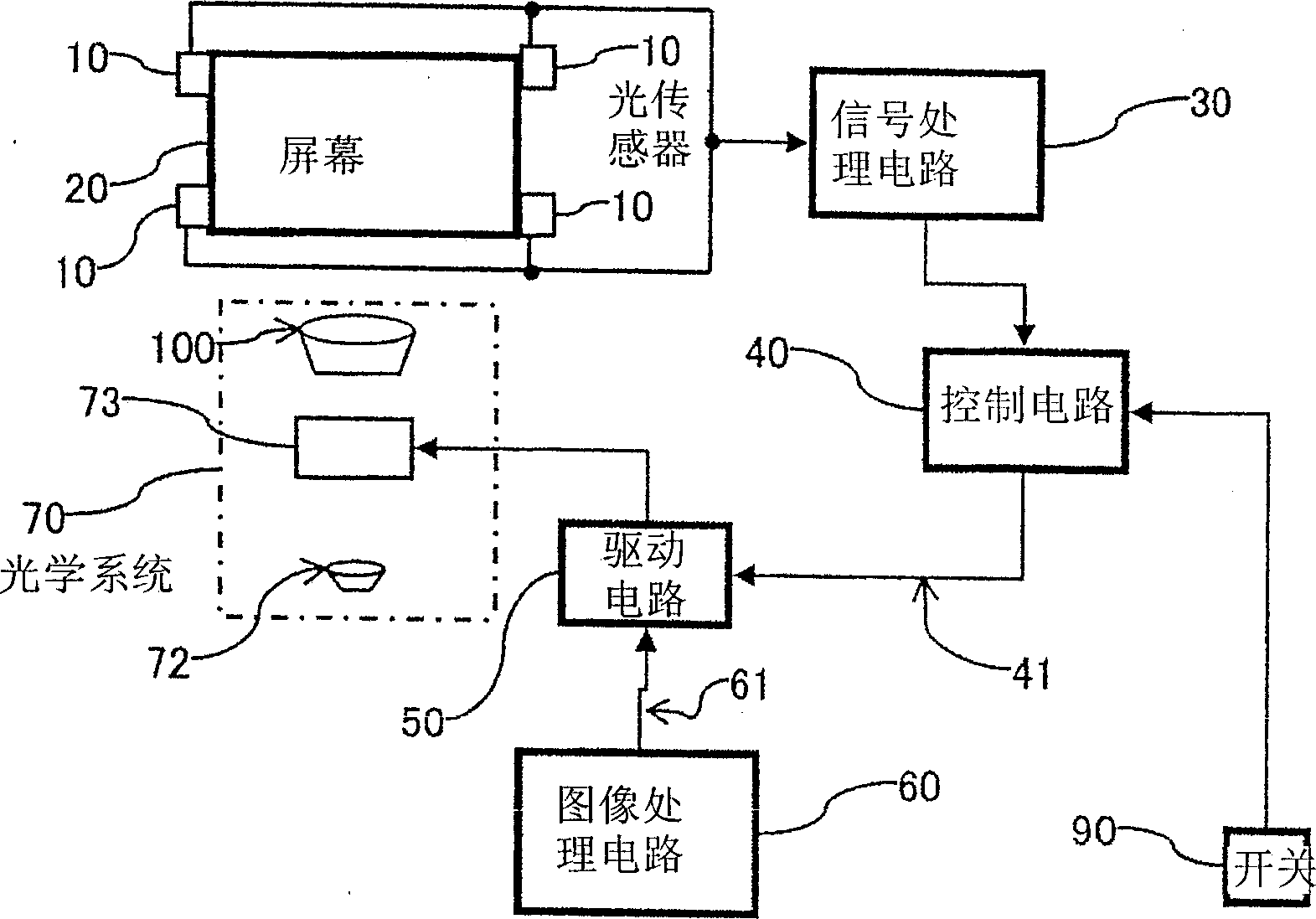
[0031] figure 1 It is a block diagram showing the configuration of the liquid crystal display device of the first embodiment. Figure 4 It is a figure which shows the control flow of a control circuit. Figure 7 It is a configuration diagram of a signal processing circuit.

[0032] exist figure 1 Among them, the liquid crystal display device is an image processing circuit 60 that performs predetermined image processing on an unillustrated image signal; it is used to adjust the The test pattern that flickers and drives the driving circuit 50 of liquid crystal display element 73; The light from light source 72 corresponds to the driving signal from driving circuit 50 on liquid crystal display element 73 and carries out the modulation of light intensity and will form the optical image ( For illustration) after being enlarged with the projection lens 100, projected onto the optical system 70 on the screen 20; The photosensor 10 of part of the nearby image light; the signal pro...

Embodiment 2

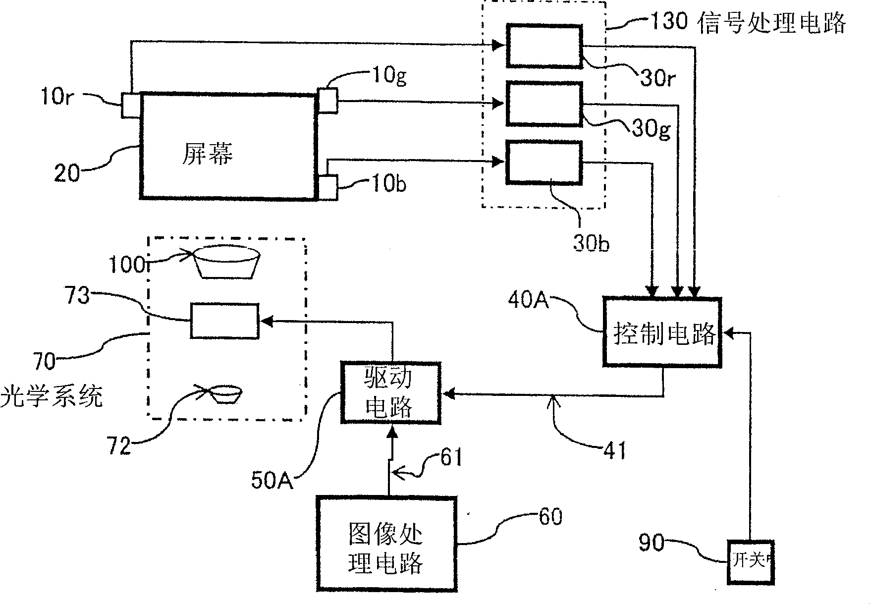
[0050] In the first embodiment, the flicker adjustment of the liquid crystal display element corresponding to the first color (for example, red) is performed, next, the flicker adjustment of the liquid crystal display element corresponding to the second color (for example, green) is performed, and finally, The flicker adjustment of the liquid crystal display element corresponding to the third color (for example, blue) is performed, but it takes time to perform such flicker adjustment. Therefore, the second embodiment in which the flicker adjustment of each color is simultaneously performed and the adjustment time is shortened will be described below.

[0051] figure 2 It is a block diagram showing the liquid crystal display device of the second embodiment. exist figure 2 in, for with figure 1 Elements with the same function are marked with the same symbols, and repeated descriptions are omitted.

[0052] exist figure 2 Among them, photosensors 10r, 10g, and 10b that re...

Embodiment 3

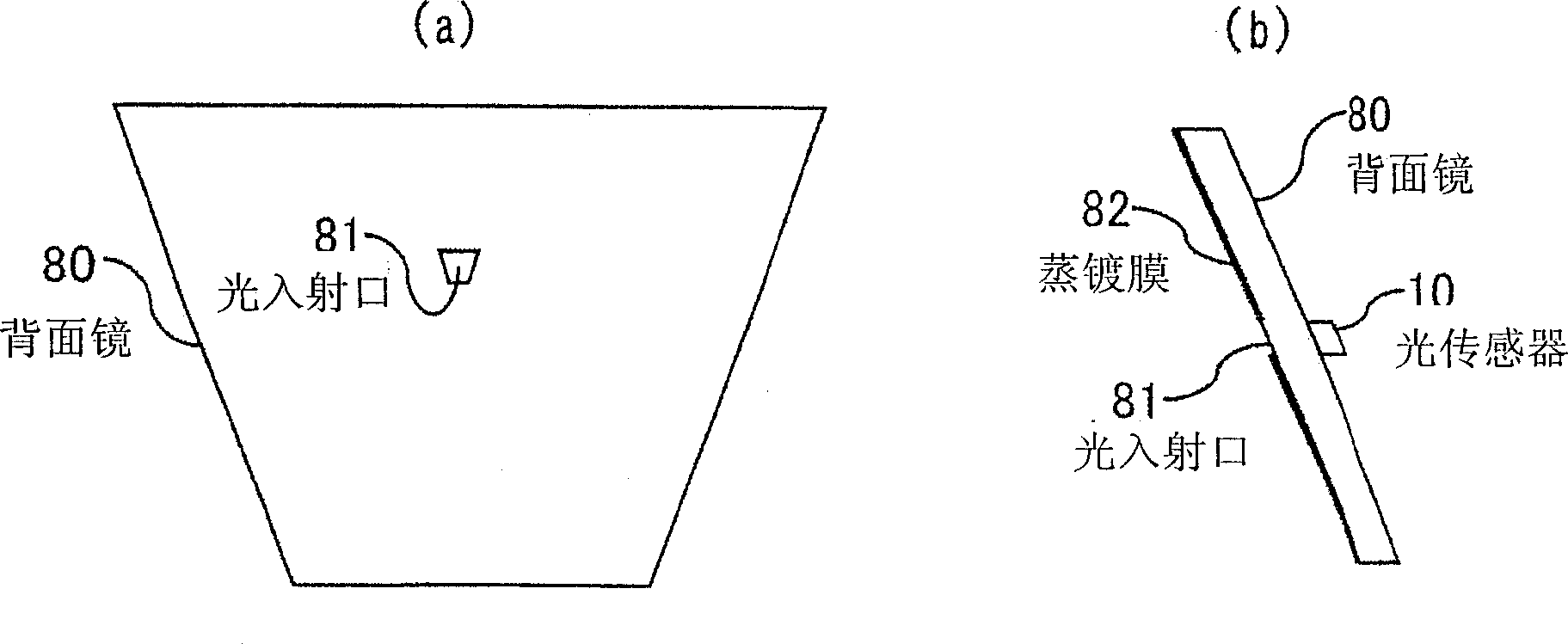
[0059] Although in the first and second embodiments, the photosensor 10 is disposed on the outer edge of the screen 20, the present invention is not limited thereto. In the first and second embodiments, the position of the photosensor is at the edge of the outer contour of the screen, so the amount of light received by the photosensor is small, and the amplitude of the output signal of the photosensor becomes smaller. Use the following image 3 In the third embodiment, an embodiment in which the optical sensor 10 is provided on the back of a rear mirror (folding mirror) used in a rear projection type liquid crystal display device will be described.

[0060] image 3 is a schematic configuration diagram of the rear mirror shown in the third embodiment, image 3 (a) is a conceptual diagram of the rear mirror 80 seen from the front, image 3 (b) is an image diagram of the rear mirror 80 seen from the lateral direction.

[0061] In this example, if image 3 As shown, the opti...


PUM


Abstract

The present invention provides an image display device capable of adjusting fluctuations in reference voltages of counter electrodes caused by aging changes in liquid crystal display elements without hindering display of input signals. In the present invention, an image display device that irradiates light from a light source onto a liquid crystal display element, forms an optical image corresponding to an image signal, and enlarges and projects it is provided with a reflector that reflects light irradiated onto the liquid crystal display element. mirror, a light sensor provided on the reflection mirror to detect light intensity, a drive circuit to drive the liquid crystal display element, and a control circuit to control the drive circuit based on the light intensity detected by the light sensor.

Description

technical field [0001] The invention relates to an image display device which enlarges and projects the image of a display element on a screen to form an image. Background technique [0002] In an active matrix liquid crystal display element (liquid crystal display panel), for example, used in a display device, an AC voltage inverted in a field period or a line period is applied between a pixel electrode and a counter electrode. However, the characteristics of the transistor for driving the pixel electrode vary, and the DC electrode of the counter electrode deviates from the inversion center voltage, causing flicker in the liquid crystal display element. In order to prevent the occurrence of such flicker, Patent Document 1 describes a technology for automatically adjusting the reference voltage applied to the counter electrode before shipment. [0003] In addition, Patent Document 2 describes a technique for automatically adjusting the common electrode voltage by detecting ...

Claims


Application Information

Patent Timeline
Patent Type & Authority Applications(China)
IPC IPC(8): G09G3/36G02F1/133G09G3/20
Inventor 坂口义弘牧野一仁岩佐浩吉泽和彦吉田秀树
Owner HITACHI LTD
Why Eureka
Try Eureka