Method and system for inspecting semiconductor defect

A technology for semiconductor and defect testing, applied in the field of defect detection, which can solve problems such as inability to clearly know location information and reduced production capacity

Inactive Publication Date: 2006-11-01
POWERCHIP SEMICON CORP
View PDF0 Cites 2 Cited by
  • Summary
  • Abstract
  • Description
  • Claims
  • Application Information

AI Technical Summary

Problems solved by technology

[0006] However, because the above method needs to go through two FBM tests, and the chip burn-in test also takes a lot of time, it will lead to a decrease in production capacity.
In addition, the above method still cannot clearly know the position information of the bad bits generated for each defect test

Method used


Image

  • Method and system for inspecting semiconductor defect
  • Method and system for inspecting semiconductor defect
  • Method and system for inspecting semiconductor defect

Examples


Embodiment Construction

[0024] In order to make the above and other objects, features and advantages of the present invention more comprehensible, preferred embodiments are listed below and described in detail with accompanying drawings.

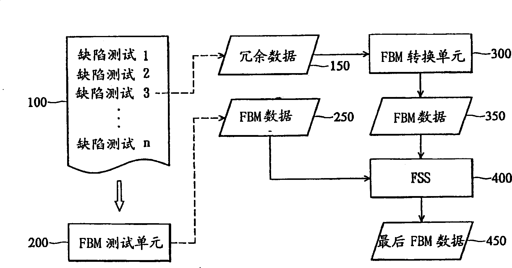
[0025] The embodiment of the present invention discloses a defect detection method and system using bad bitmap (FBM).

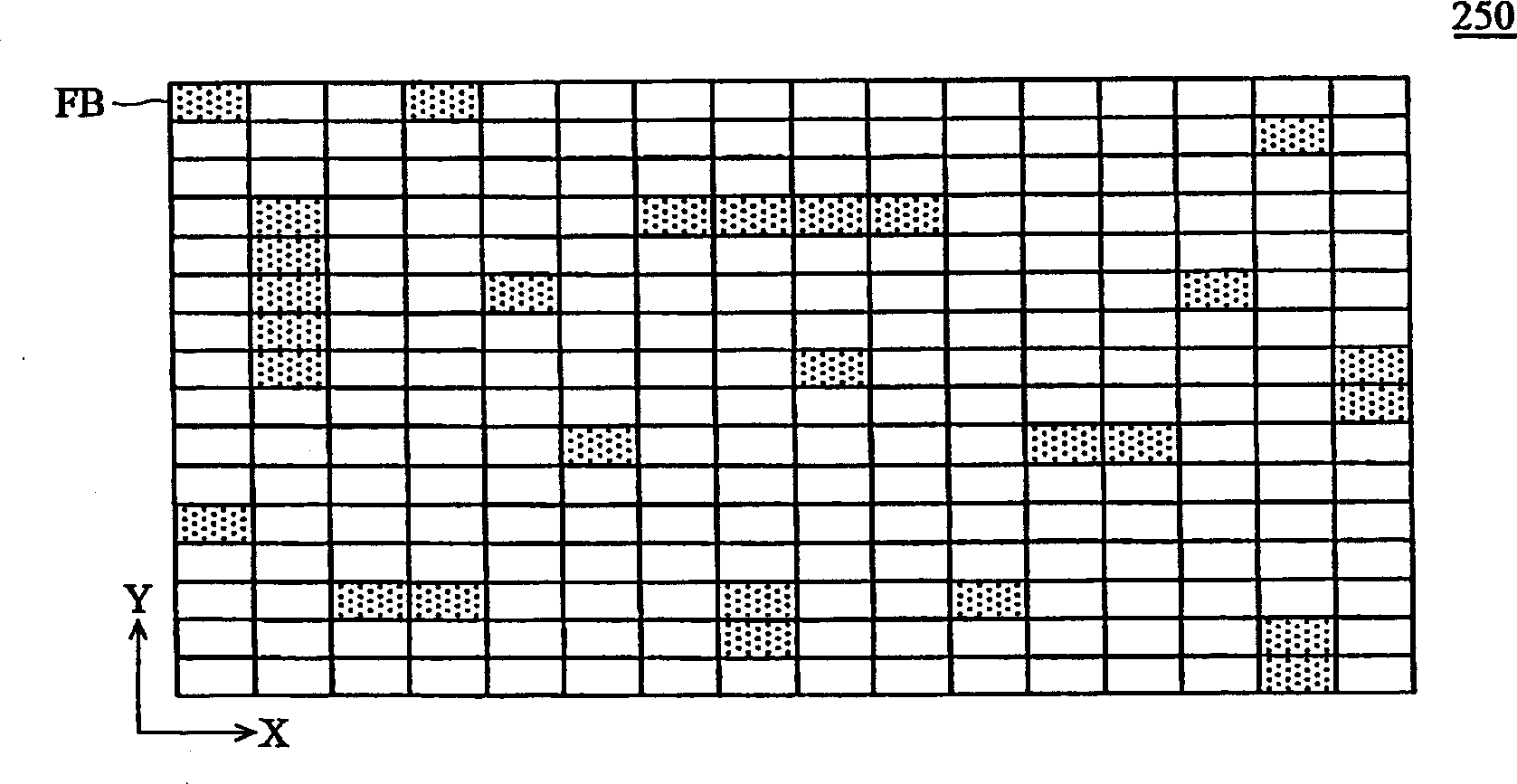
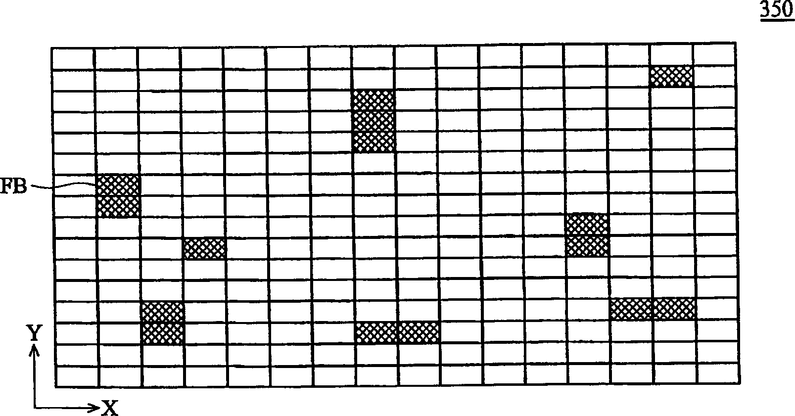
[0026] When performing the FBM test, it records all the bad bits of the chip and forms a bad bit map in the form of a matrix. As mentioned above, performing two FBM tests can find out the position information of the defective bits corresponding to the defect tests performed between the two FBM tests. The position information of the bad bits generated by the test is identified and analyzed, and the chip cannot be selected arbitrarily. Based on this point, the embodiment of the present invention stores redundancy information (ie, defect information) generated during each defect test, and then converts the redundancy information into data compatible...


PUM


Abstract

The invention is designed for use in testing defect of wafer in a process of manufacturing semiconductor and comprises the following steps: executing an operation for testing defect and getting its redundant information; executing an operation for testing the abnormal state and getting a first bad bit-mapping; the redundant information is converted to a second bad bit-mapping; comparing the first bad bit-mapping with the second bad bit-mapping to generate a third bad bit-mapping.

Description

technical field [0001] The invention relates to a defect detection method, in particular to a defect detection method for finding wafer defects by using a FailBit Map (FBM for short). Background technique [0002] In terms of semiconductor technology, it can be mainly divided into integrated circuit (Integrated Circuit, IC for short) design, wafer fabrication (Wafer Fabrication, Wafer Fab for short), wafer testing (Wafer Probe), and wafer packaging (Packaging). Wafer testing is to test each grain (grain) on the chip, install a probe (probe) on the detection head, and test its electrical characteristics by contacting the contact (pad) on the grain. Unqualified grains will be Marked, and then when the chip is cut into individual dies in units of dies, the marked unqualified dies will be eliminated, and the next process will not be carried out, so as not to increase the manufacturing cost. [0003] Wafer testing is mainly to find out the defects on the chip. Traditionally, all...

Claims


Application Information

Patent Timeline
Patent Type & Authority Applications(China)
IPC IPC(8): H01L21/66G01N21/88
Inventor 张延生刘东昱
Owner POWERCHIP SEMICON CORP
Why Eureka
Try Eureka