Method of manufacturing a multilayer semiconductor structure with reduced ohmic losses

A multi-layer structure, semiconductor technology, applied in the direction of semiconductor devices, semiconductor/solid-state device manufacturing, waveguides, etc., can solve the problems of electrical performance deterioration and harmfulness of multi-layer structures

Inactive Publication Date: 2006-11-01
ЮНІВЕРСИТЕ КАТОЛІК ДЕ ЛУВЕН
View PDF0 Cites 18 Cited by
  • Summary
  • Abstract
  • Description
  • Claims
  • Application Information

AI Technical Summary

Problems solved by technology

Since these losses deteriorate the electrical properties of multilayer structures, especially for high-frequency applications, they are considered detrimental

Method used


Image

  • Method of manufacturing a multilayer semiconductor structure with reduced ohmic losses
  • Method of manufacturing a multilayer semiconductor structure with reduced ohmic losses
  • Method of manufacturing a multilayer semiconductor structure with reduced ohmic losses

Examples


preparation example Construction

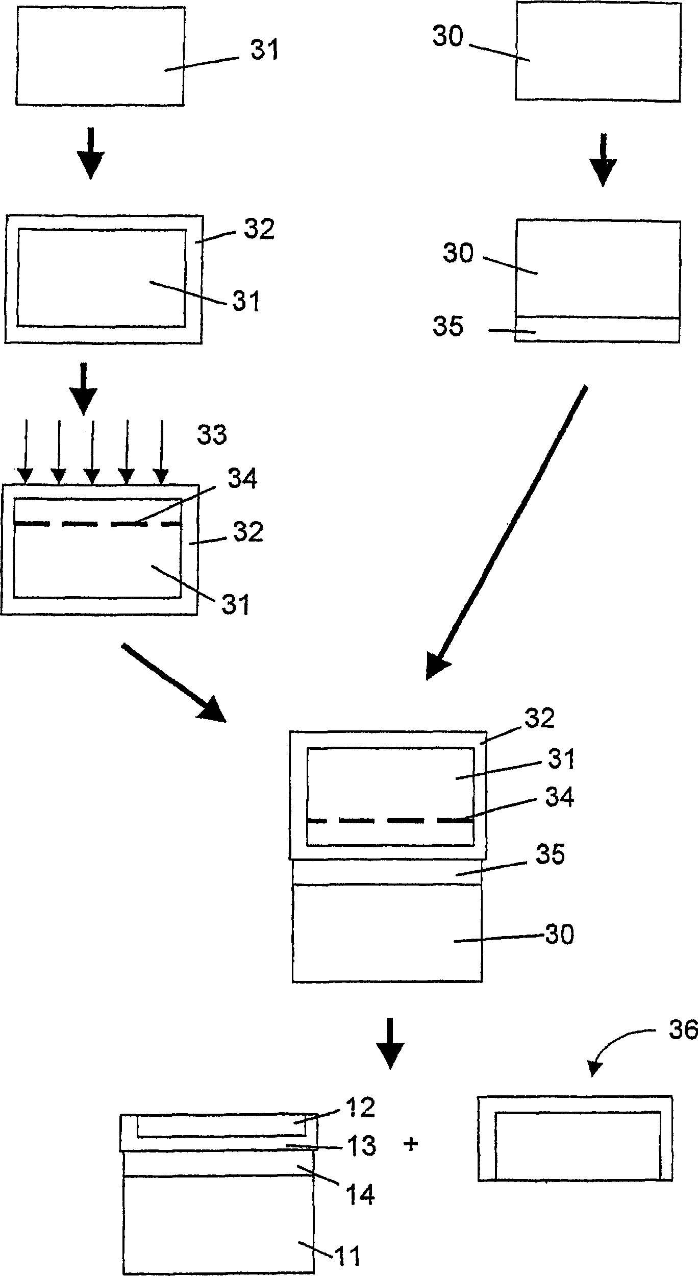
[0070] - Preparation of structures.

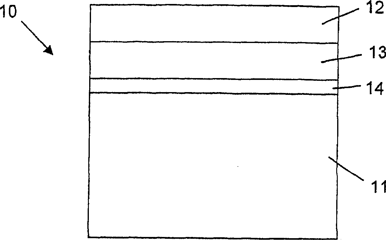
[0071] - Selective etching of the active layer 12 of the structure, which in the case of SOI may stop at the insulating layer 13 of buried oxide.

[0072] - Deposition of the entire conductive metal layer on the structure on top of the buried oxide.

[0073] - Selective dry etching of deposited metal to form detection patterns, in this case conductive parallel metal lines forming a coplanar waveguide (CPW), between which there is a central metal line.

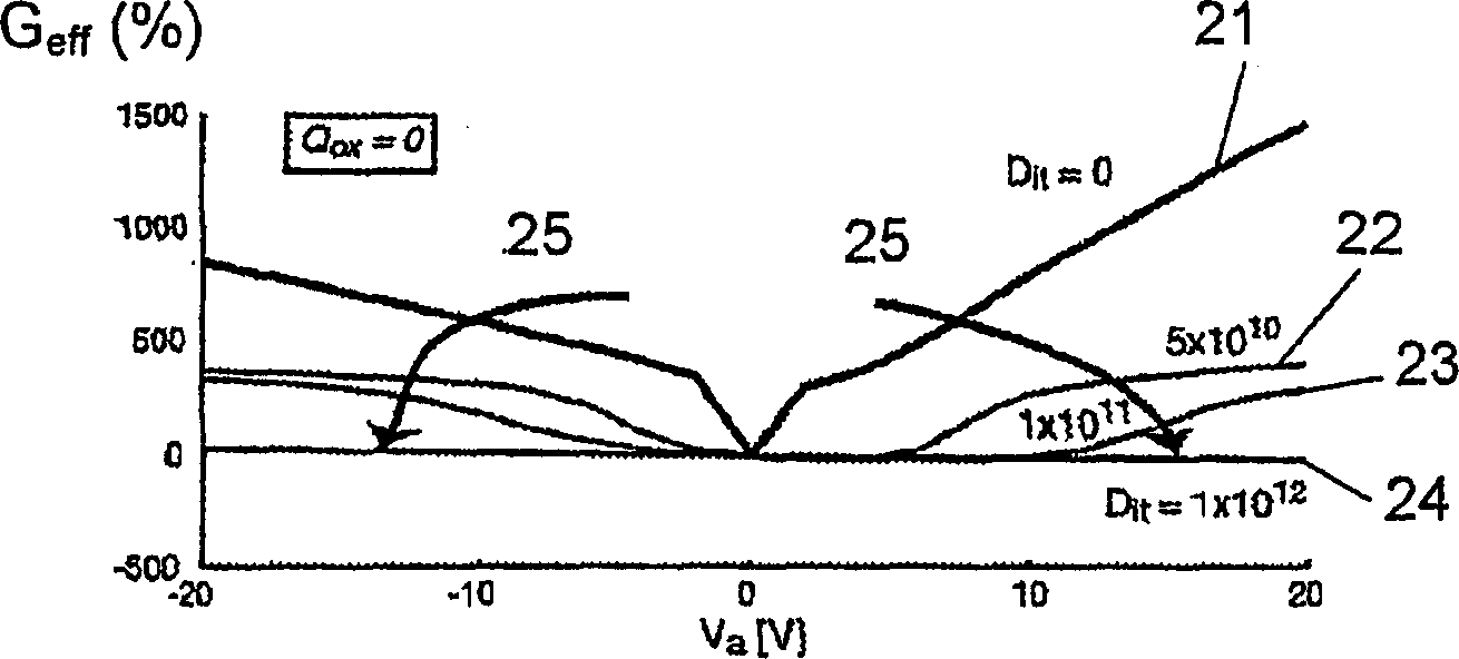
[0074] - Application of an electrical signal on the central wire. The signal consists of a superposition of low-amplitude continuous and alternating voltages. This combined voltage is applied to the wires and the following parameters can be determined:

[0075] - Amplitude V of the continuous component A ,

[0076] - frequency f of the alternating component.

[0077] The superimposition of continuous and alternating voltage components during the measurement shows that the low-conducti...


PUM


Abstract

The present invention provides a method of manufacturing a multilayer semiconductor structure featuring reduced ohmic losses with respect to standard multilayer semiconductor structures. The semiconductor structure comprises a high resistivity silicon substrate with resistivity higher than 3 Kohm.cm, an active semiconductor layer and an insulating layer in between the silicon substrate and the active semiconductor layer. The method comprises suppressing ohmic losses inside the high resistivity silicon substrate by increasing, with regard to prior art devices, charge trap density between the insulating layer and the silicon substrate. In particular this may be obtained by applying an intermediate layer in between the silicon substrate and the insulating layer, the intermediate layer comprising grains having a size, wherein the mean size of the grains of the intermediate layer is smaller than 150 nm, preferably smaller than 50 nm.

Description

(1) Technical field [0001] The present invention relates to a method of fabricating a multilayer semiconductor structure comprising a high resistivity (HR) silicon substrate, an active semiconductor layer, and an insulating layer between the silicon substrate and the active semiconductor layer. The invention also relates to the multilayer semiconductor structures thus obtained. In particular, the present invention relates to multilayer semiconductor structures suitable for use in high frequency (HF, ie operating at frequencies above 100 MHz) integrated circuits, such as radio frequency (RF), and methods of manufacturing the same. (2) Background technology [0002] A multilayer semiconductor structure includes a plurality of layers, at least some of which are made of different materials. [0003] An example of such a multilayer semiconductor structure is a silicon-on-insulator (SOI) structure. SOIs include: [0004] Thin (tens of nanometers up to several micrometers) activ...

Claims


Application Information

Patent Timeline
Patent Type & Authority Applications(China)
IPC IPC(8): H01L21/762H01P3/00
CPCH01L21/76254H01L2223/6627H01L2924/1903H01P3/006H01L21/02002H01L21/70H01L21/762
Inventor D·莱德拉J·P·拉斯金
Owner ЮНІВЕРСИТЕ КАТОЛІК ДЕ ЛУВЕН
Why Eureka
Try Eureka