Adhesive tape peeling device

A technology of peeling device and adhesive tape, applied in the directions of adhesives, transportation and packaging, electric solid devices, etc., can solve the problem of low efficiency and so on

Inactive Publication Date: 2006-11-22
LINTEC CORP
View PDF2 Cites 3 Cited by
  • Summary
  • Abstract
  • Description
  • Claims
  • Application Information

AI Technical Summary

Problems solved by technology

[0010] However, in the above-mentioned peeling method, it is necessary to use air blowing, suction, adhesive tape and other peeling mechanisms to remove each shrunk and bent surface protection tape from the surface of the plate-shaped member, because this operation must be performed manually. , so the problem of low efficiency

Method used


Image

  • Adhesive tape peeling device
  • Adhesive tape peeling device
  • Adhesive tape peeling device

Examples


Embodiment Construction

[0064] Hereinafter, embodiments of the present invention will be described with reference to the drawings.

[0065]

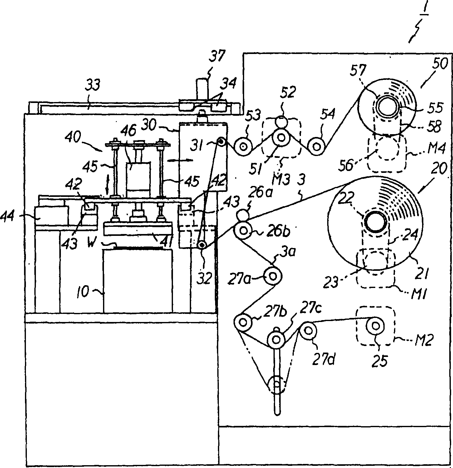
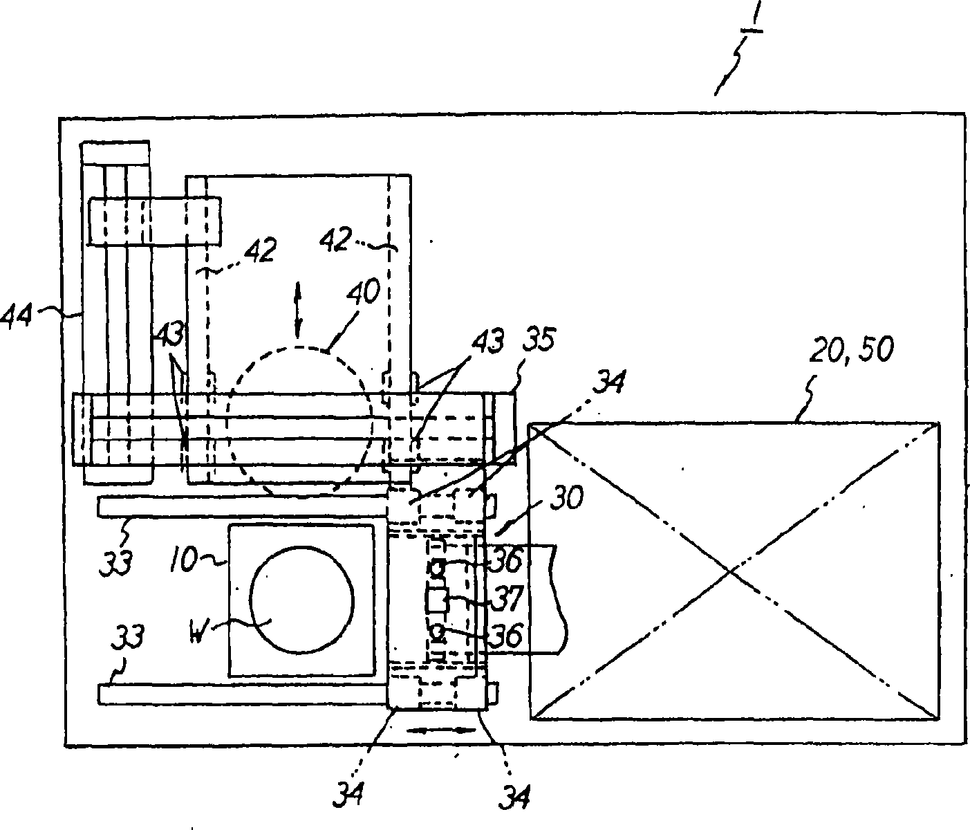
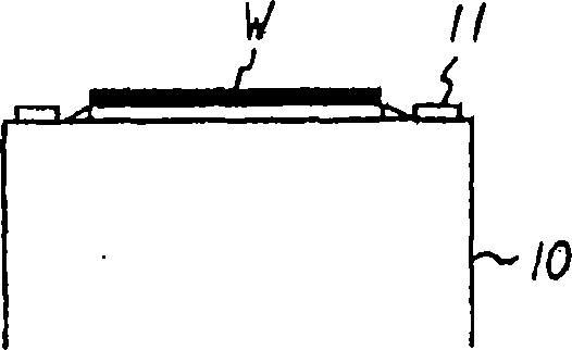
[0066] figure 1 is a side view of the peeling device according to Embodiment 1 of the present invention, figure 2 Yes figure 1 A top view of the stripping device, image 3 Yes figure 1 Side view of the adsorption table portion of the stripping device, Figure 4 is a top view of the adsorption table part, Figure 5 is a cross-sectional view of a wafer with a surface protection tape (adhesive tape) attached to its surface, Image 6 It is a sectional view of a surface protection tape (adhesive tape).

[0067] The peeling device 1 of the present embodiment is used in the semiconductor manufacturing process from Figure 5 The surface of the shown wafer W with the singulated surface protection tape 2 a stuck thereto has the singulated surface protection tape 2 a peeled off from the surface.

[0068] In this embodiment, when a specific circuit pattern is fo...


PUM


Abstract

An adhesive tape peeling device capable of easily and efficiently peeling adhesive tape formed into pieces from a plate-like member. The device for peeling a surface protective tape(2a) formed into chip sizes and stuck on the surface of a wafer W comprises a peeling tape supply means (20) delivering a peeling tape (3) to the wafer W set on a suction table (10), a peeling tape sticking means sticking the peeling tape (3) delivered by the peeling tape supply means (20) on the entire surface of the surface protective tape (2a) stuck on the surface of the wafer W, a heating means heating, together with the adhesive tape, the peeling tape stuck on the entire surface of the adhesive tape by the peeling tape sticking means, a tape peeling means peeling off, together with the peeling tape, the adhesive tape adhered to the peeling tape by heating by the heating means from the plate-like member, and a collecting means collecting the adhesive tape peeled off from the plate-like member by the tape peeling means and the peeling tape.

Description

technical field [0001] The present invention relates to a device for peeling an adhesive tape such as a surface protection tape from a plate-shaped member, and the adhesive tape is formed into individual pieces according to the chip size and attached to the surface of a plate-shaped member such as a semiconductor wafer. Background technique [0002] For example, in the semiconductor chip manufacturing process of the electronics industry or the optical industry, when a predetermined circuit pattern is formed on the surface of the semiconductor wafer (hereinafter referred to as the wafer), in order to make the thickness of the wafer uniform or to remove the circuit formed For the oxide film, the back surface of the wafer is polished, and then the wafer is diced (singulated) for each circuit to manufacture semiconductors. [0003] However, grinding dust is generated when the wafer is ground, and once the grinding dust touches the circuit pattern, the circuit pattern may be dama...

Claims


Application Information

Patent Timeline
Patent Type & Authority Applications(China)
IPC IPC(8): B65H41/00B29C63/00B65H37/00H01L21/00H01L21/68H01L21/78
CPCB29C63/0013B65H37/002B65H2701/192H01L21/67132H01L21/6835H01L2221/6834H01L2221/68395Y10T156/19Y10T156/1911
Inventor 明地武志
Owner LINTEC CORP
Why Eureka
Try Eureka