Circuit arrangement for supplying configuration data in FGPA devices
一种电路布置、配置数据的技术,应用在使用特定组件的逻辑电路、使用基本逻辑电路组件的逻辑电路、逻辑电路等方向,能够解决增大电路开支等问题
- Summary
- Abstract
- Description
- Claims
- Application Information
AI Technical Summary
Problems solved by technology
Method used
Image

Examples
Embodiment Construction
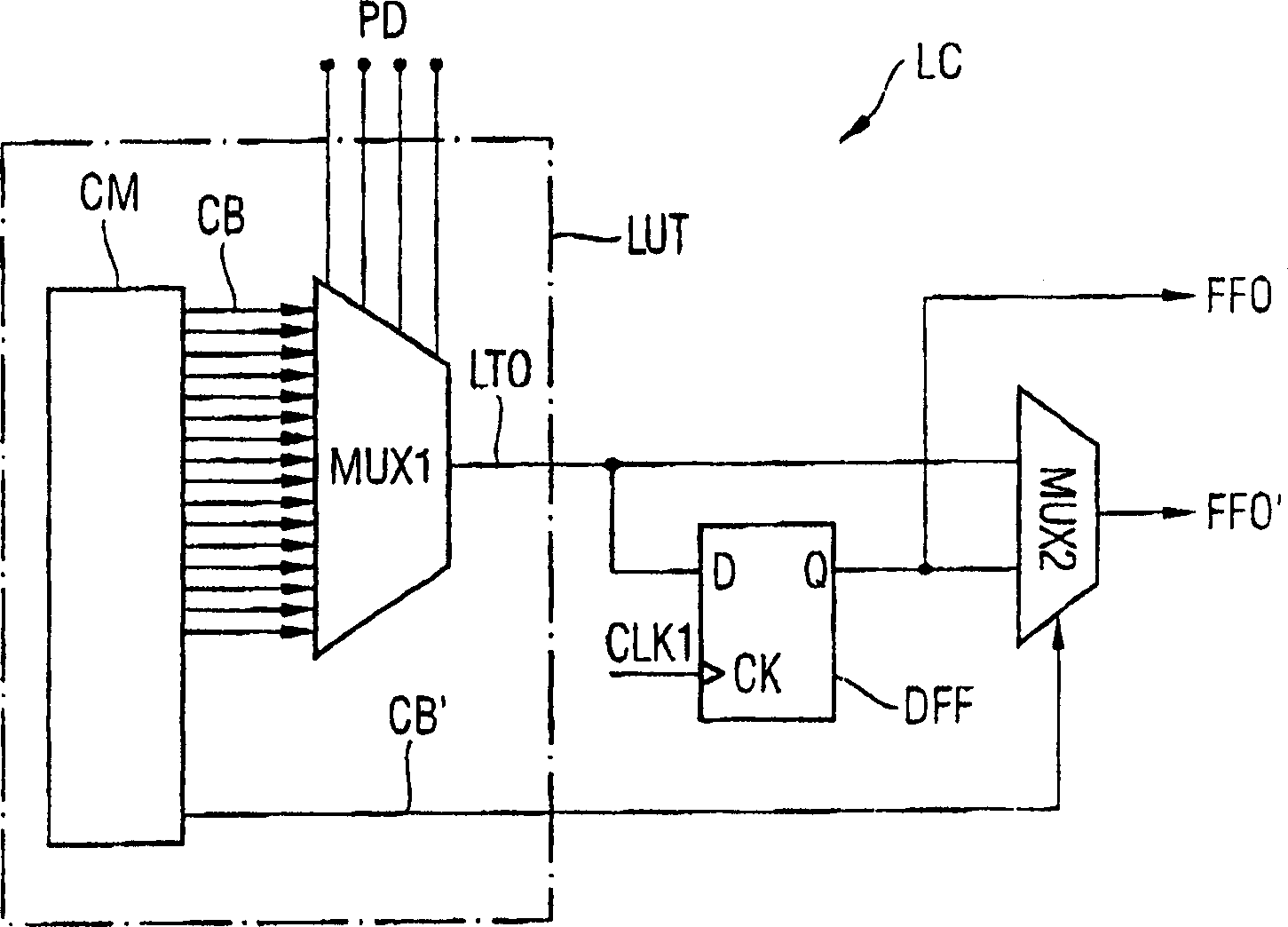
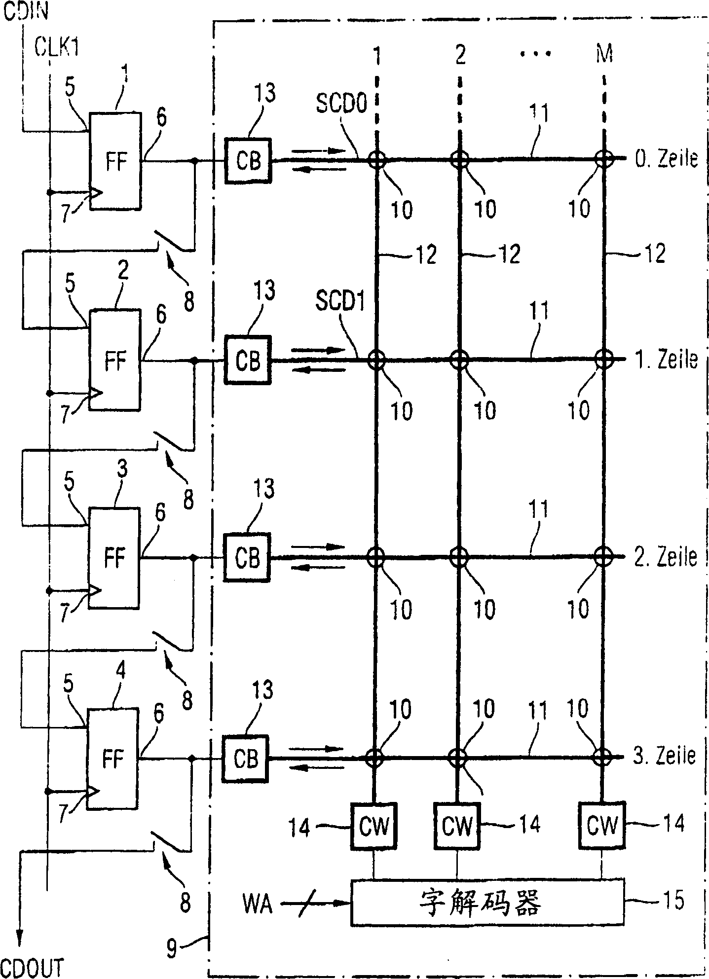
[0048] image 3 A first embodiment of an interconnect according to the invention is shown having an output flip-flop coupled to a non-volatile memory of an associated configurable logic cell. Several flip-flops 1 , 2 , 3 , 4 arranged in a column are shown, each having a data input 5 , a data output 6 and a clock input 7 . The shown flip flops 1 , 2 , 3 , 4 are in each case part of a programmable logic unit (not shown here in more detail). For example in figure 1 In the operation according to the prior art shown and provided in , the flip-flops 1, 2, 3, 4 are used as output flip-flops to output the output signal of the look-up table of the corresponding logic unit.
[0049] According to the invention, the data input 5 of the first flip-flop 2 is in each case switchably connected via a switch 8 to the data output 6 of the second output flip-flop 1 . A common clock signal CLK is supplied to the clock input 7 of the output flip-flops 1 , 2 , 3 , 4 . Furthermore, a memory cell ...
PUM
 Abstract
Description
Claims
Application Information
 - R&D
- Intellectual Property
- Life Sciences
- Materials
- Tech Scout
- Unparalleled Data Quality
- Higher Quality Content
- 60% Fewer Hallucinations
Browse by: Latest US Patents, China's latest patents, Technical Efficacy Thesaurus, Application Domain, Technology Topic, Popular Technical Reports.
© 2025 PatSnap. All rights reserved.Legal|Privacy policy|Modern Slavery Act Transparency Statement|Sitemap|About US| Contact US: help@patsnap.com