

LCD panel and method for manufacturing same
A liquid crystal display, liquid crystal layer technology, applied in nonlinear optics, instruments, optics, etc., can solve problems such as inability to ensure accuracy, and achieve high-precision effects
- Summary
- Abstract
- Description
- Claims
- Application Information
AI Technical Summary
Problems solved by technology
Method used
Image

Examples
Embodiment Construction
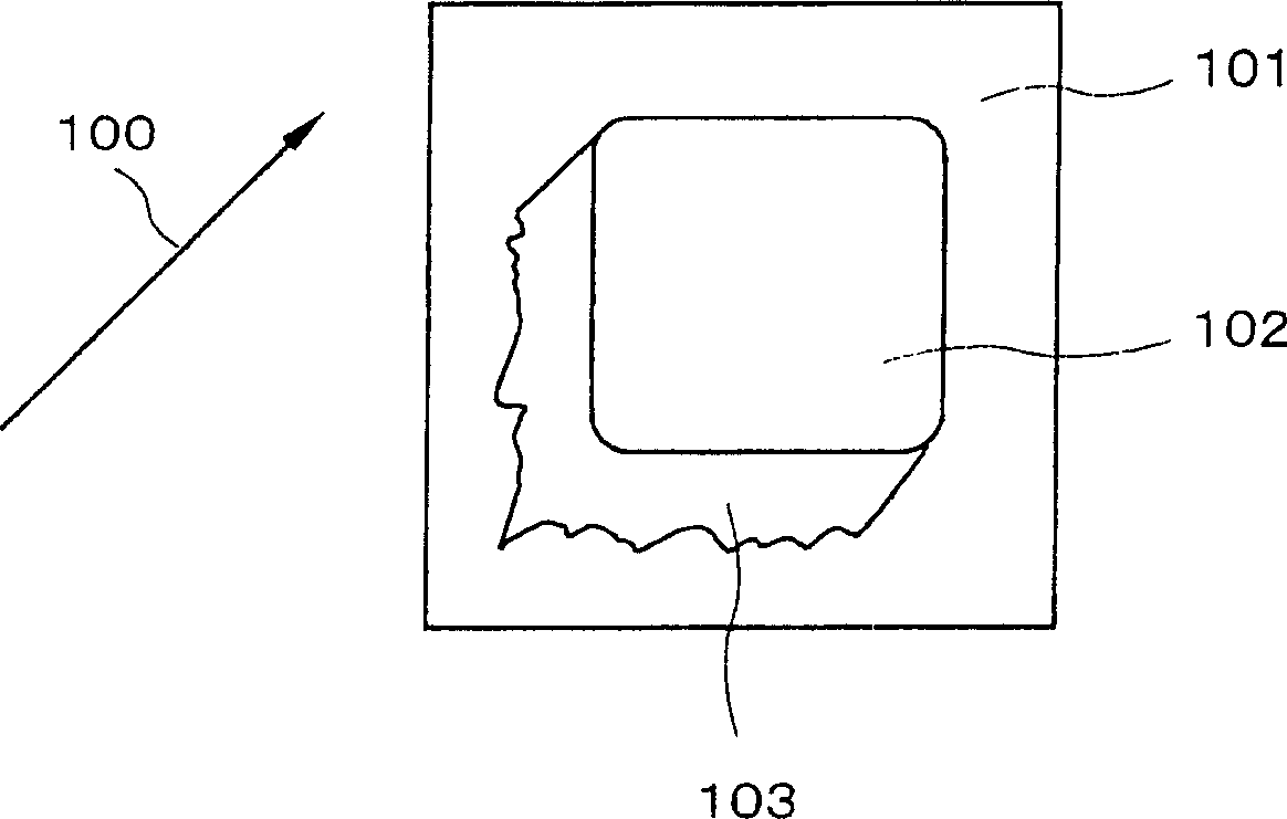
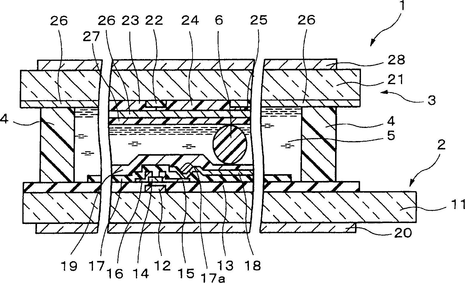
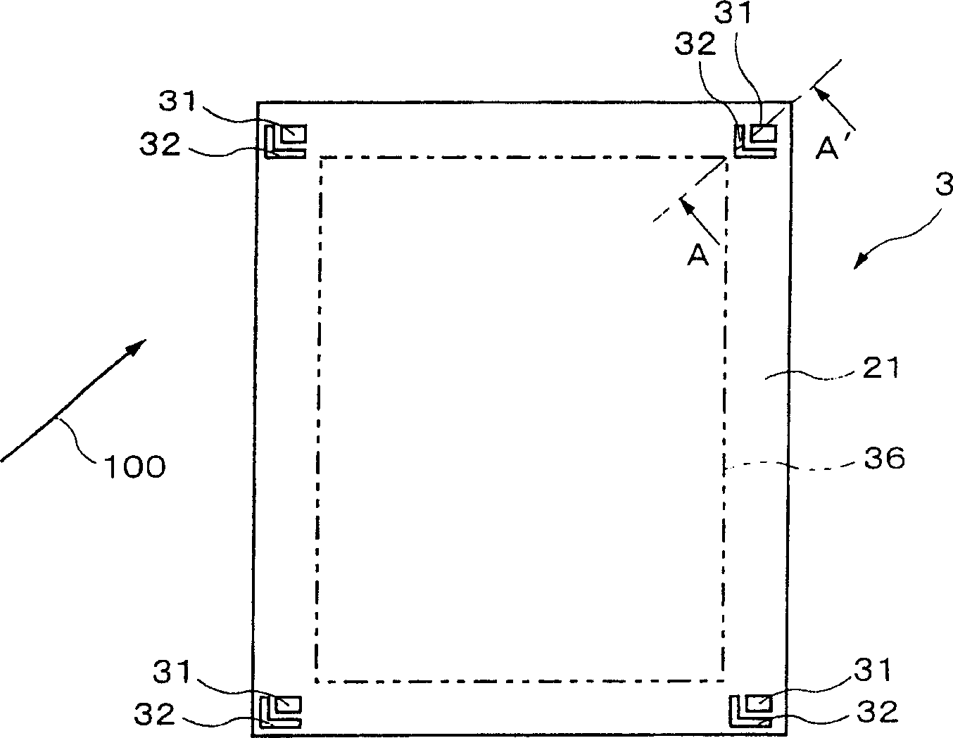
[0036] Hereinafter, embodiments of the present invention will be described in detail with reference to the accompanying drawings. A first embodiment of the present invention will be described first. figure 2 A cross-sectional view of the LCD according to the present embodiment is shown; image 3 A plan view of the CF substrate of the present LCD is shown; Figure 4 show image 3 Plan view of the alignment marks and capture pattern of the CF substrate shown; Figure 5 is along image 3 a cross-sectional view along line A-A' as shown; and Figure 6 show Figure 4 Perspective view of alignment marks and capture graphic shown.
[0037] Such as figure 2 As shown, in the LCD panel 1 according to the present embodiment, a TFT substrate 2 and a color filter (CF) substrate 3 are arranged parallel to each other, and a frame-shaped sealing member 4 is arranged between the TFT substrate 2 and the CF substrate 3, to surround the display area of the LCD panel 1 . Liquid crystals ...
PUM
| Property | Measurement | Unit |
|---|---|---|
| angle | aaaaa | aaaaa |
| thickness | aaaaa | aaaaa |
| thickness | aaaaa | aaaaa |
Abstract
Description
Claims
Application Information