MOS transistor with partial depletion SOI structure and producing method thereof

A technology of MOS transistors and manufacturing methods, which is applied in the field of new structure MOS transistors and their manufacturing, can solve the problems of SOIMOS transistors, such as limited gate-to-channel control capability, limited scaling capability, difficulty in integrated circuits, etc., to achieve strong short-channel Effect suppression capability, elimination of harsh requirements, effect of barrier punchthrough suppression

Inactive Publication Date: 2007-01-03
PEKING UNIV SHENZHEN GRADUATE SCHOOL +1
View PDF0 Cites 10 Cited by
  • Summary
  • Abstract
  • Description
  • Claims
  • Application Information

AI Technical Summary

Problems solved by technology

However, due to the limited control ability of the gate to the channel of this partially depleted SOI MOS transistor, the short-channel effect is serious, and the ability to scale down is limited. At the same time, this type of device also has a serious Kink effect, which makes this type of device It is also difficult to apply to the production of integrated circuits at the nanoscale

Method used


Image

  • MOS transistor with partial depletion SOI structure and producing method thereof
  • MOS transistor with partial depletion SOI structure and producing method thereof
  • MOS transistor with partial depletion SOI structure and producing method thereof

Examples


Embodiment Construction

[0051]The specific embodiments described below in conjunction with the accompanying drawings help to understand the features and advantages of the present invention, but the implementation of the present invention is by no means limited to the described embodiments.

[0052] A specific embodiment of the manufacturing method of the present invention includes Figure 1 to Figure 10 Process steps shown:

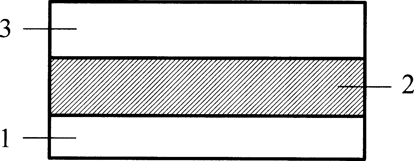
[0053] 1. If figure 1 As shown, the SOI substrate silicon wafer is prepared, and the SOI substrate silicon wafer structure includes a silicon substrate (1), a buried oxide layer (2) and a silicon film (3), and the shallow trench isolation (STI) technology is used on the silicon film ( 3) An active region is formed on the top;

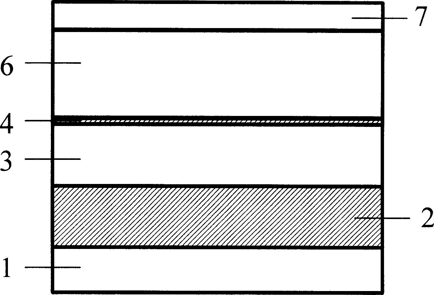
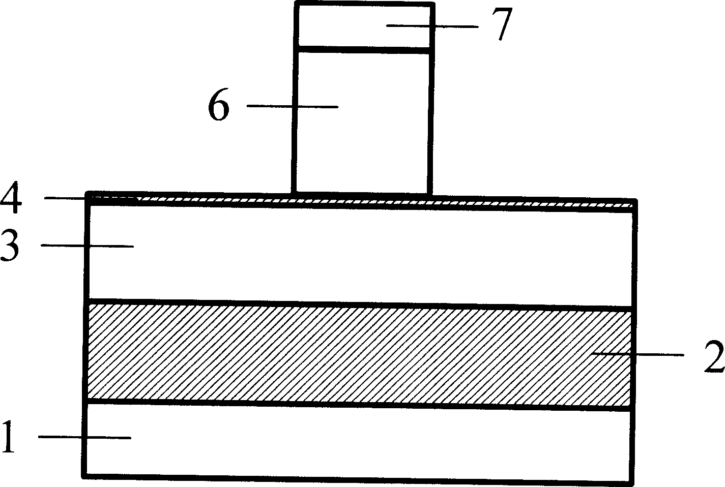
[0054] 2. If figure 2 As shown, the gate dielectric layer silicon dioxide (4) is grown by a thermal oxidation method, and the thickness of the gate dielectric layer silicon dioxide (4) is in the range of 1-10nm; then, a 100nm gate electrode layer poly...


PUM


Abstract

The present invention provides part depletion SOI constructional MOS transistor used in nano integrated circuit manufacturing technology and making method. The upper part of said transistor source drain expansion zone is thin semiconductor layer, the lower part being cavity unit, said structure having advantages of ultrathin unit all depletion SOI MOS transistor and partial depleted SOI MOS transistor and overcoming their shortage. Said invented preparation method is compatible with traditional MOS transistor making technology, with simple technological process and use value.

Description

Technical field: [0001] The invention belongs to the technical field of semiconductor integrated circuits and its manufacture, and in particular relates to a MOS transistor with a new structure and a manufacturing method thereof. Background technique: [0002] The feature size of MOS transistors continues to scale down. When entering the nanometer scale, various small size effects such as short channel effect (SCE) and drain-induced barrier lowering effect (DIBL) become more and more serious, and the serious impact is small. Device Performance of Dimensional MOS Transistors. Therefore, in order to continue to maintain the strong scaling ability of MOS transistors at the nanometer scale, researchers have proposed a variety of new structures, new materials and new processes. [0003] Silicon-on-insulator (SOI) devices are one such device. According to the thickness of the silicon film, SOI devices are mainly divided into two categories: [0004] One type is a fully depleted...

Claims


Application Information

Patent Timeline
Patent Type & Authority Applications(China)
IPC IPC(8): H01L29/78H01L21/336
Inventor 张盛东李定宇韩汝琦王新安张天义
Owner PEKING UNIV SHENZHEN GRADUATE SCHOOL
Why Eureka
Try Eureka