Memory system and method of accessing memory chips of a memory system

A storage chip and storage system technology, applied in the field of storage systems, can solve the problems that the storage chip cannot be accessed in advance and the power consumption increases.

Inactive Publication Date: 2007-01-10
INFINEON TECH AG
View PDF0 Cites 4 Cited by
  • Summary
  • Abstract
  • Description
  • Claims
  • Application Information

AI Technical Summary

Problems solved by technology

[0009] b) memory chips cannot be accessed in advance for certain setup procedures or for certain power-related procedures;
[0010] c) The memory chip cannot be accessed independently of the command and data flow;
[0011] d) According to figure 1 memory chips in a shared ring topology and according to figure 2 The main memory chip 210 in the star topology of must utilize the row and column selection included in the protocol to distinguish between redrive and memory chip read / write procedures, which results in higher logic effort;
[0012] e) Since the row and column selection command and clock enable information must be decoded when they are included in the protocol, even if only one redrive has to be performed in the memory chip, it involves body, therefore power dissipation increases

Method used


Image

  • Memory system and method of accessing memory chips of a memory system
  • Memory system and method of accessing memory chips of a memory system
  • Memory system and method of accessing memory chips of a memory system

Examples


Embodiment Construction

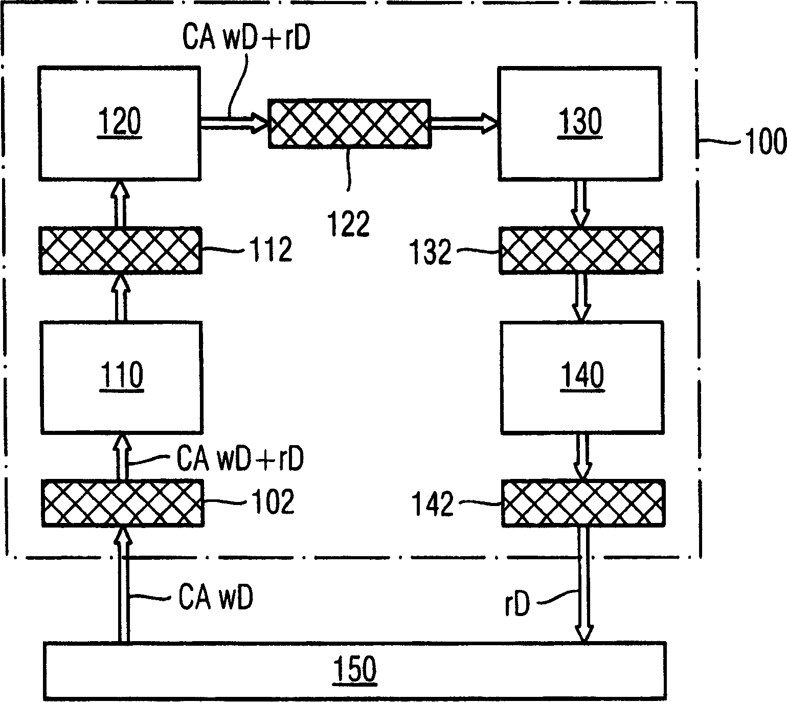
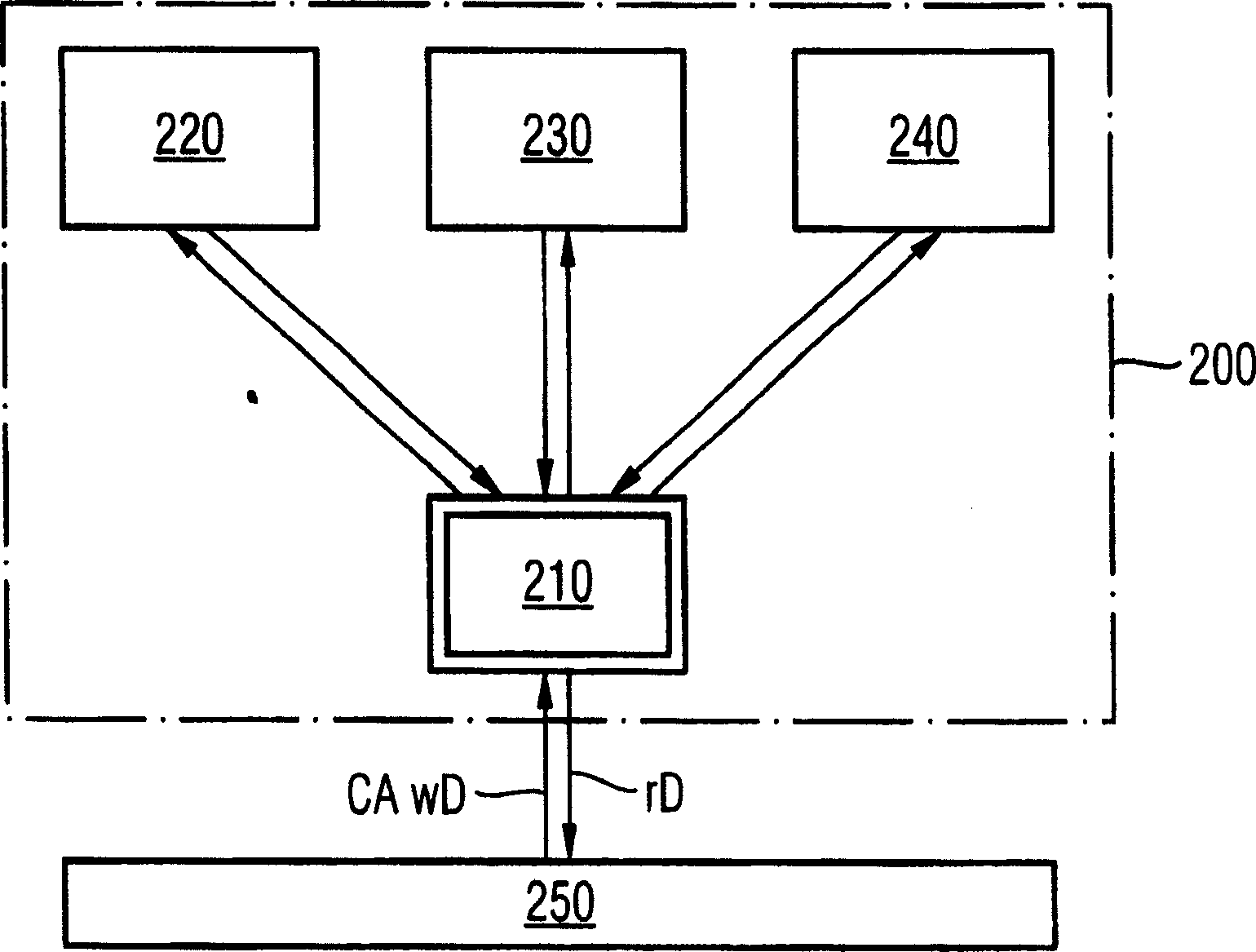
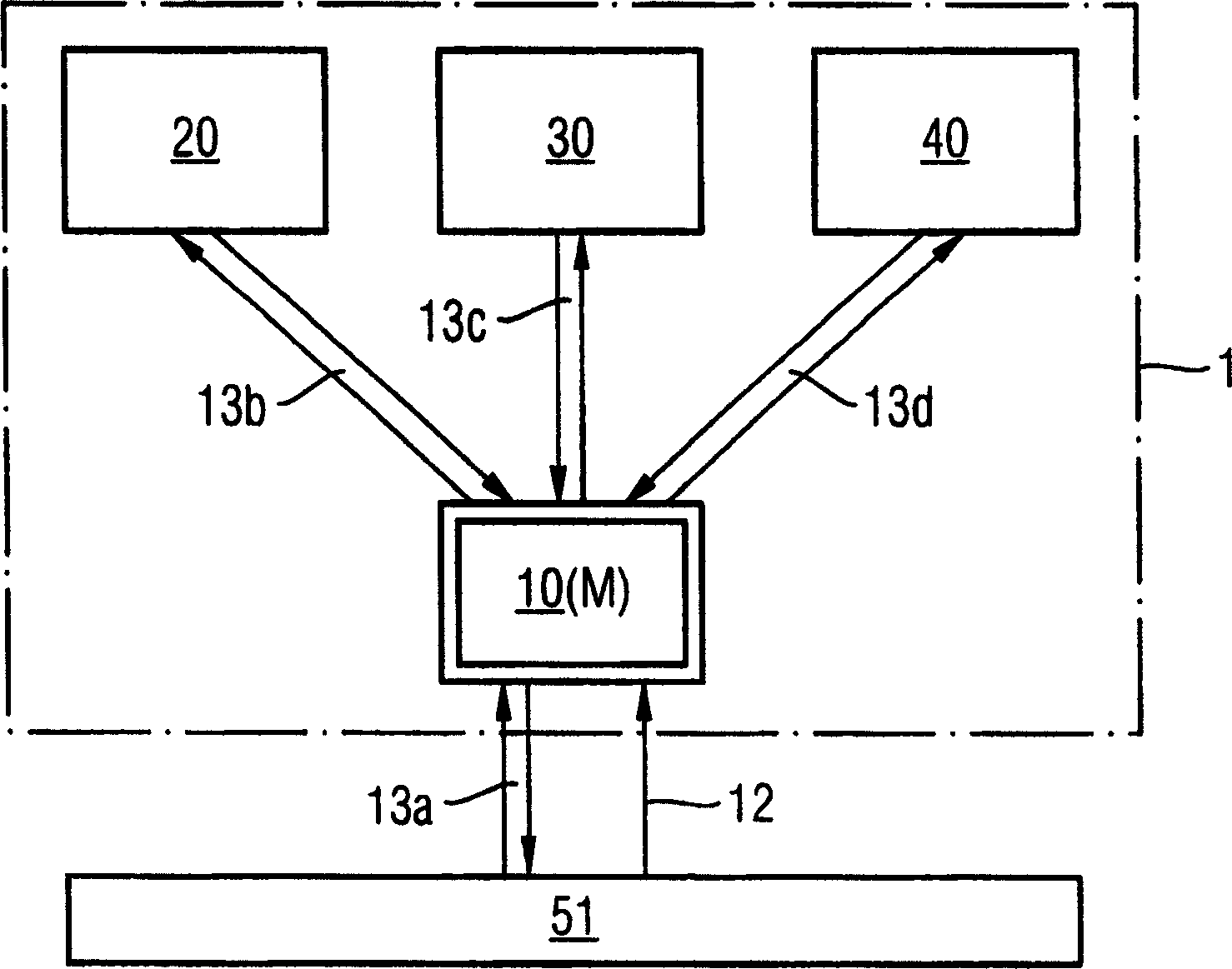
[0022] In the following detailed description, reference is made to the accompanying drawings, which form a part hereof, and in which are shown by way of illustrations specific embodiments in which the invention may be practiced. In this regard, directional terms such as "top", "bottom", "front", "rear", "leading", "trailing", etc. are used with reference to the orientation of the Figures shown. Since components of embodiments of the present invention may be positioned in a number of different orientations, directional terminology is used for purposes of illustration and is in no way limiting. It is to be understood that other embodiments may be utilized and structural or logical changes may be made without departing from the scope of the present invention. Accordingly, the following detailed description should not be read in a limiting sense, but rather the scope of the invention is defined by the appended claims.

[0023] In one embodiment, the present invention provides a m...


PUM


Abstract

A memory system and method is disclosed. In one embodiment, the memory system includes a memory controller and at least one memory module on which a certain number of semiconductor memory chips and connecting lines are arranged in a respectively specified topology. The connecting lines include first connecting lines forming transfer channels for a protocol based transfer of data and command signal streams from the memory controller to at least one of the memory chips on the memory module and from there to the memory controller, respectively. Second connecting lines are routed separately from the memory controller directly to at least one of the memory chips on the memory module for transferring select information to the at least one memory chip separately from the data and command signal streams.

Description

technical field [0001] The present invention relates to a memory system comprising a memory controller and at least one memory module on which a certain number of semiconductor memory chips and connection lines are arranged in a specific topology, and to a method for this A method for accessing semiconductor memory chips of a memory system. Background technique [0002] Recent developments in fast semiconductor memories will lead to high-speed signal transfer rates of eg up to 7 Gbit / s. These high signaling rates require careful design considerations in terms of the implementation of a suitable topology and the proper method of accessing from the memory controller to the memory chips on the memory module. [0003] attached figure 1 Depicts a functional block diagram of an example of a heretofore known shared ring structure, which is a possibility of how to arrange a certain number of memory chips (eg, DRAM chips) on the memory module 100 in consideration of the connection ...

Claims


Application Information

Patent Timeline
Patent Type & Authority Applications(China)
IPC IPC(8): G11C11/34
CPCG11C5/063G06F12/00G06F13/14
Inventor P·瓦尔纳R·施勒兹P·格雷戈里乌斯H·鲁克鲍尔
Owner INFINEON TECH AG
Why Eureka
Try Eureka