Display array, multi-layer complementary wire structure and mfg. method

A manufacturing method and display technology, applied in semiconductor/solid-state device manufacturing, electrical components, circuits, etc., can solve problems such as time delay and display quality

Inactive Publication Date: 2007-01-31
IND TECH RES INST
View PDF0 Cites 4 Cited by
  • Summary
  • Abstract
  • Description
  • Claims
  • Application Information

AI Technical Summary

Problems solved by technology

As mentioned above, as the size of the panel increases, the length of the metal connection in the thin film transistor display will also increase significantly, and the resistance...

Method used


Image

  • Display array, multi-layer complementary wire structure and mfg. method
  • Display array, multi-layer complementary wire structure and mfg. method
  • Display array, multi-layer complementary wire structure and mfg. method

Examples


Embodiment Construction

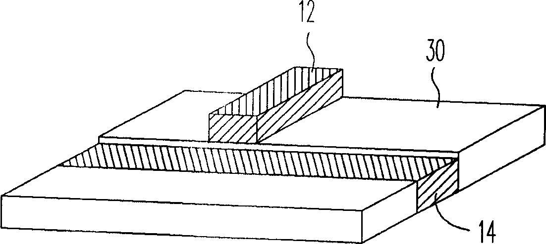
[0092] Figures 4A-4G It is a cross-sectional view of the manufacturing process of a conventional thin film transistor. First, please refer to Figure 4A The manufacturing method of the thin film transistor is to first form the metal layer M1 on the substrate 410. The substrate 410 can be a silicon substrate, a glass substrate or a plastic substrate, etc., and the metal layer can be a conductive metal material such as aluminum metal or copper metal. . Then use the first photolithography mask Mask-1 to pattern the metal layer M1 by means of photolithography and etching to form a gate (gate) 420 on the substrate 410 . Next, please refer to Figure 4B , forming a gate insulating layer, an active layer and a doped layer on the substrate 410 sequentially and comprehensively. The forming method is, for example, depositing (Deposition) an insulating layer (Insulating Layer) 430 , an amorphous silicon layer (Amorphous Silicon, “a-Si”) 440 and an ohmic contact layer (Ohmic Contact ...


PUM


Abstract

The invention relates to a display array, a multilayer complementary lead structure and the manufacturing method thereof, on the condition of not increasing photo-masks, manufacturing a thin film transistor (TFT) display array with multilayer complementary lead structure, able to solve the problem of lead resistance in a display unit.

Description

technical field [0001] The present invention relates to a wire structure and manufacturing method and a thin film transistor display array manufacturing method, and in particular to a multi-layer complementary wire structure and manufacturing method that can solve the problem of wire resistance and a multi-layer complementary wire structure. Manufacturing method of thin film transistor display array. Background technique [0002] As the size of the panel increases, the length of the metal connection in the thin film transistor display will also increase significantly, and the resulting considerable time delay becomes a major problem in display quality. Most of the existing 37-inch LCD TV panels have a panel ratio of 16:9, and the RC delay time (RC delay time) of the metal connection derived from the length of the scanning line will seriously affect the picture quality. Most panel manufacturers solve the resistance-capacitance delay phenomenon with a double-sided driving met...

Claims


Application Information

Patent Timeline
IPC IPC(8): H01L21/84H01L21/768
Inventor 陈昱丞陈麒麟张启明
Owner IND TECH RES INST
Why Eureka
Try Eureka