Solid-state imaging device and portable electronic apparatus with the same

A technology of solid-state imaging devices and electronic equipment, which is applied to televisions, installations, electrical components, etc., can solve the problems of no DSP configuration and higher height of solid-state imaging devices, and achieve the effect of saving space

Inactive Publication Date: 2007-02-07
SEIKO PRECISION CO LTD
View PDF2 Cites 2 Cited by
  • Summary
  • Abstract
  • Description
  • Claims
  • Application Information

AI Technical Summary

Problems solved by technology

However, in the solid-state imaging device of Japanese Patent Application No. 2003-182018, there is no description about the arrangement of the DSP.
Therefore, if Figure 12 When the DSP is arranged on the back side of the substrate on which the solid-state imaging device is mounted on the front side as shown, there is a problem that the height of the solid-state imaging device in the direction of the optical axis becomes high due to the thickness of the DSP.

Method used


Image

  • Solid-state imaging device and portable electronic apparatus with the same
  • Solid-state imaging device and portable electronic apparatus with the same
  • Solid-state imaging device and portable electronic apparatus with the same

Examples


Embodiment 1

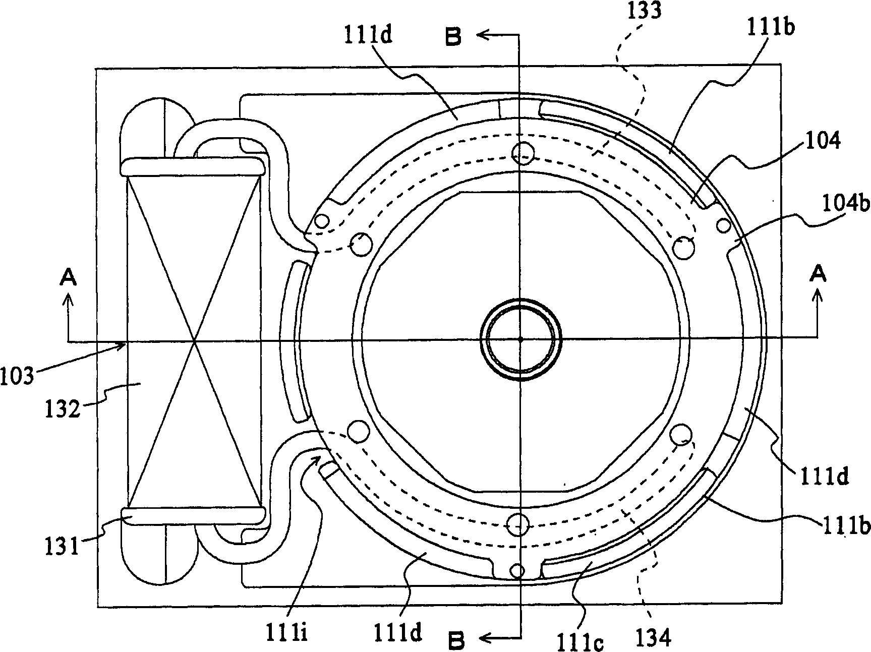
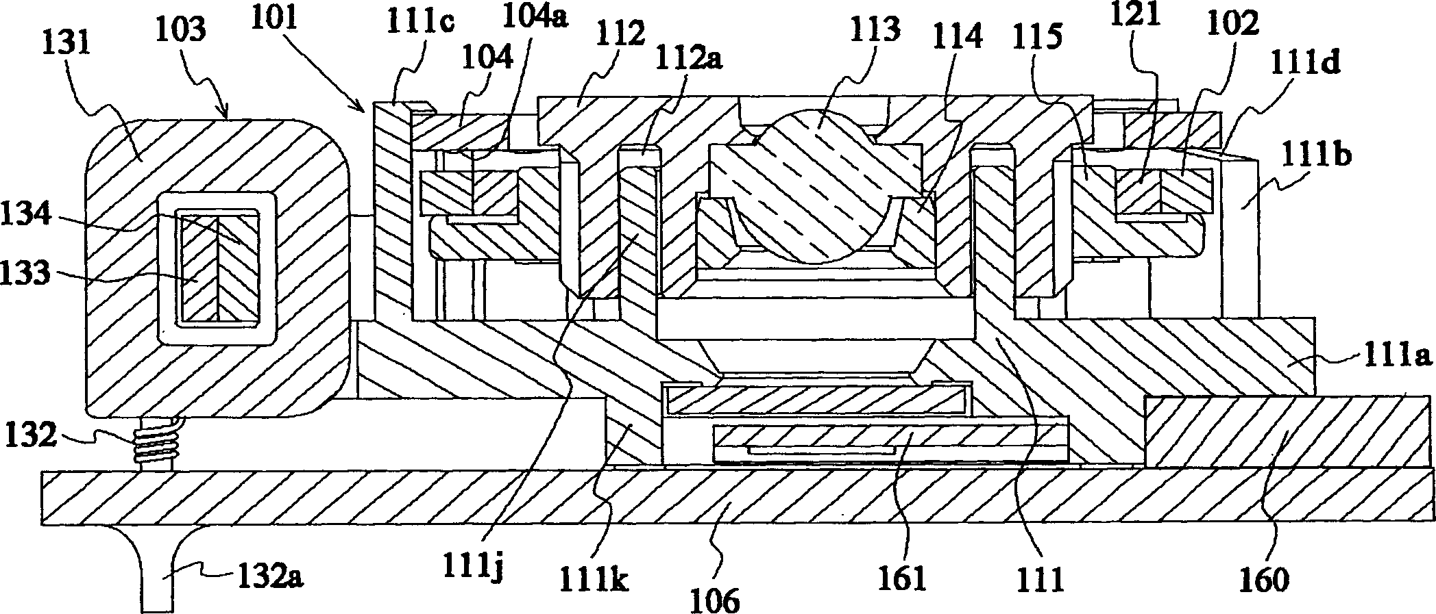
[0036] First, refer to figure 1 and figure 2 The configuration of this embodiment will be described. In addition, in figure 1 , shows a top view of the solid-state imaging device of the present invention, in figure 2 is shown along the figure 1 The shape of the section cut by the line AA shown.

[0037] like figure 2 As shown, the solid-state imaging device of this embodiment has: a substrate 106 on which an imaging element 161 composed of a CCD or the like is mounted; and a lens unit 101 mounted on the substrate 106 and holding a Lens 113 on element 161. The lens unit 101 includes: a bracket 111, which is fixed on the substrate 106 in a manner surrounding the imaging element 161; a lens holder 112, which is engaged with the bracket 111 in a manner that can move along the optical axis direction of the lens 113, and is used to hold the lens 113 and an electromagnetic drive unit (driver), which drives the lens holder 112 to a first position and a second position, th...

Embodiment 2

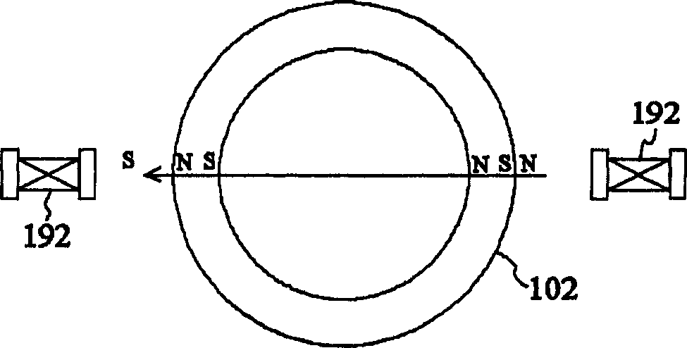
[0062] Next, refer to Figure 9 , 10 A second embodiment of the present invention will be described. This embodiment also has: a substrate 106 on which an imaging element 161 made of a CCD or the like is installed; 113. The lens unit 101 includes: a bracket 111, which is fixed on the substrate 106 in a manner surrounding the imaging element 161; a lens bracket 112, which is engaged with the bracket 111 in a manner that can move along the optical axis of the lens 113, and is used to hold the lens 113; and a rotating member 221 as a lens position adjusting member (driving portion) that drives the lens holder 112 to a first position and a second position that is moved a predetermined distance from the first position in the direction of the optical axis s position.

[0063] An adjustment member 220 is provided on the outer periphery of the cylindrical lens holder 112 . The mounting position of the adjustment member 220 and the lens holder 112 is adjusted by rotating the lens ...


PUM


Abstract

A solid-state imaging device having a circuit board (106) on which an imaging device (161) is mounted and a lens unit (101) that movably holds a lens (113) and is erected on the circuit board (106) by a leg section (111k), wherein a peripheral circuit device (160) is provided between the circuit board (106) and the lens unit (101). As a result, the height of the imaging device is lower in the direction of the optical axis than a case where the peripheral circuit device (160) is provided on the circuit board (106), on the side opposite the side on which the lens unit (101) is provided.

Description

technical field [0001] The present invention relates to a solid-state imaging device that captures images using an imaging element, and more particularly to a solid-state imaging device that has a macro (close-up) imaging function in addition to a normal imaging function. Background technique [0002] Conventionally, a so-called digital camera in which an image of a subject is imaged by an optical lens on an imaging element including a CCD (Charge Coupled Device) or the like has been widely used. Various types of digital cameras have been proposed, but if so-called macro photography, in which a subject is captured within tens of centimeters, can be easily realized, it will be highly useful. In order to perform macro photography, it is necessary to change the lens position compared to the case of photographing subjects at a distance of several meters or more. [0003] As a device for changing the position of the lens, it is known to manually or electrically move the lens hol...

Claims


Application Information

Patent Timeline
Patent Type & Authority Applications(China)
IPC IPC(8): G02B7/04G02B7/08H04N5/225
CPCH04N5/2254G02B7/08H04N23/55
Inventor 甘粕幹夫
Owner SEIKO PRECISION CO LTD
Why Eureka
Try Eureka