

Manufacturing method of printed circuit board
A technology for printed circuit boards and manufacturing methods, applied in the direction of printed circuit manufacturing, multilayer circuit manufacturing, printed circuits, etc., to achieve the effects of ensuring integrity, reducing interlayer misalignment, and avoiding the addition of blocking blocks
- Summary
- Abstract
- Description
- Claims
- Application Information
AI Technical Summary
Problems solved by technology
Method used
Image

Examples
Embodiment 1
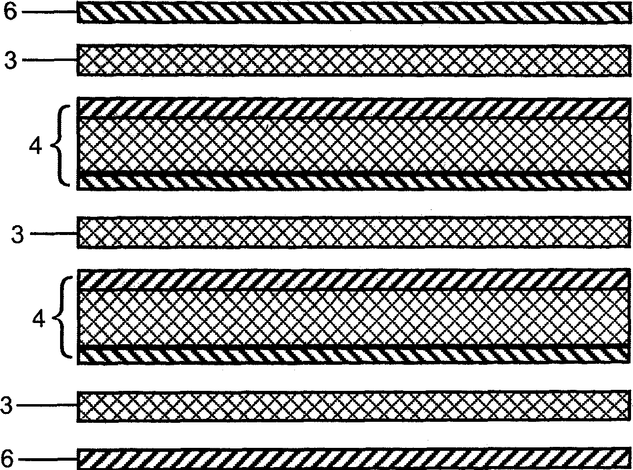
[0044] image 3 It is a schematic diagram of the stacking of six-layer boards combined with a single prepreg in Example 1 of the present invention and then locked. Figure 4 It is a flowchart of the method described in embodiment 1, comprising the steps of:
[0045] First, select and cut the core board 4 and the prepreg 3, so that the prepreg 3 is longer than the core board 4 in both length and width directions, so as to form a spare area A on the edge profile of the prepreg 3, preferably 0.5 to 1.0 inches longer on each side , the profile of the surface layer copper foil 6 is substantially the same as that of the prepreg 3;
[0046] Secondly, the prepreg 3 and a plurality of core boards 4 are alternately laminated according to the design sequence to form a laminate, wherein the upper and lower surfaces of the laminate are the prepreg 3;
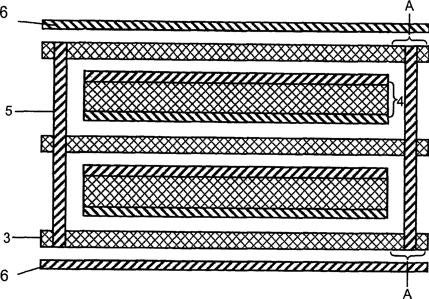
[0047] After lamination, use connectors 5 such as rivets or staples to evenly lock the edges of all the prepregs 3 of the laminate 7 in t...
Embodiment 2
[0056] Generally, when the thickness of the interlayer prepreg is 14 mils to 16 mils (mil, 1 mil=25.4×10⁻⁶m), it is necessary to connect two or more prepregs into one. An example in which two sheets of prepreg are connected as one, of course, there may be multiple sheets.
[0057] Figure 5 It is a schematic diagram of Embodiment 2 of the present invention, and two pre-locked prepregs 3 are used for lamination between six-layer boards, that is, two layers of prepregs are first connected and then laminated. Such as Figure 5 As shown, when a plurality of prepregs 3 with higher glue content are used to assemble a printed circuit board, it is basically the same as that in Example 1. Image 6 It is the flowchart of the method described in embodiment 2, comprising the steps:
[0058] First, select and cut the core board 4 and the prepreg 3, so that the prepreg 3 is longer than the core board 4 in both length and width directions, so as to form a spare area A on the edge profile ...
Embodiment 3
[0067] Figure 7 It is a schematic diagram of Embodiment 3 of the present invention, and two pre-locked prepregs 3 are directly laminated and pressed between the six-layer boards. Such as Figure 7 As shown, when a plurality of prepregs with higher glue content are used to combine printed circuit boards, it is basically the same as in Examples 1 and 2, Figure 8 It is the flowchart of the method described in embodiment 3, comprising the steps:
[0068] First, select and cut the core board 4 and the prepreg 3, so that the prepreg 3 is longer than the core board 4 in both length and width directions, so as to form a spare area A on the edge profile of the prepreg 3, preferably 0.5 to 1.0 inches longer on each side , the profile of the surface layer copper foil 6 is substantially the same as that of the prepreg 3;
[0069] Secondly, first use connecting parts 81 such as rivets or staples to evenly lock the edges of the two prepregs 3 in the spare area A to form a prepreg body;...
PUM
 Abstract
Description
Claims
Application Information