Display device and method for manufacturing display device
A technology for a display device and a manufacturing method, which is applied to lighting devices, electrical components, circuits, etc., can solve problems such as low pass rate, low production efficiency, and increased manufacturing cost, and achieve the effects of increased pass rate and improved production performance
- Summary
- Abstract
- Description
- Claims
- Application Information
AI Technical Summary
Problems solved by technology
Method used
Image

Examples
no. 1 approach
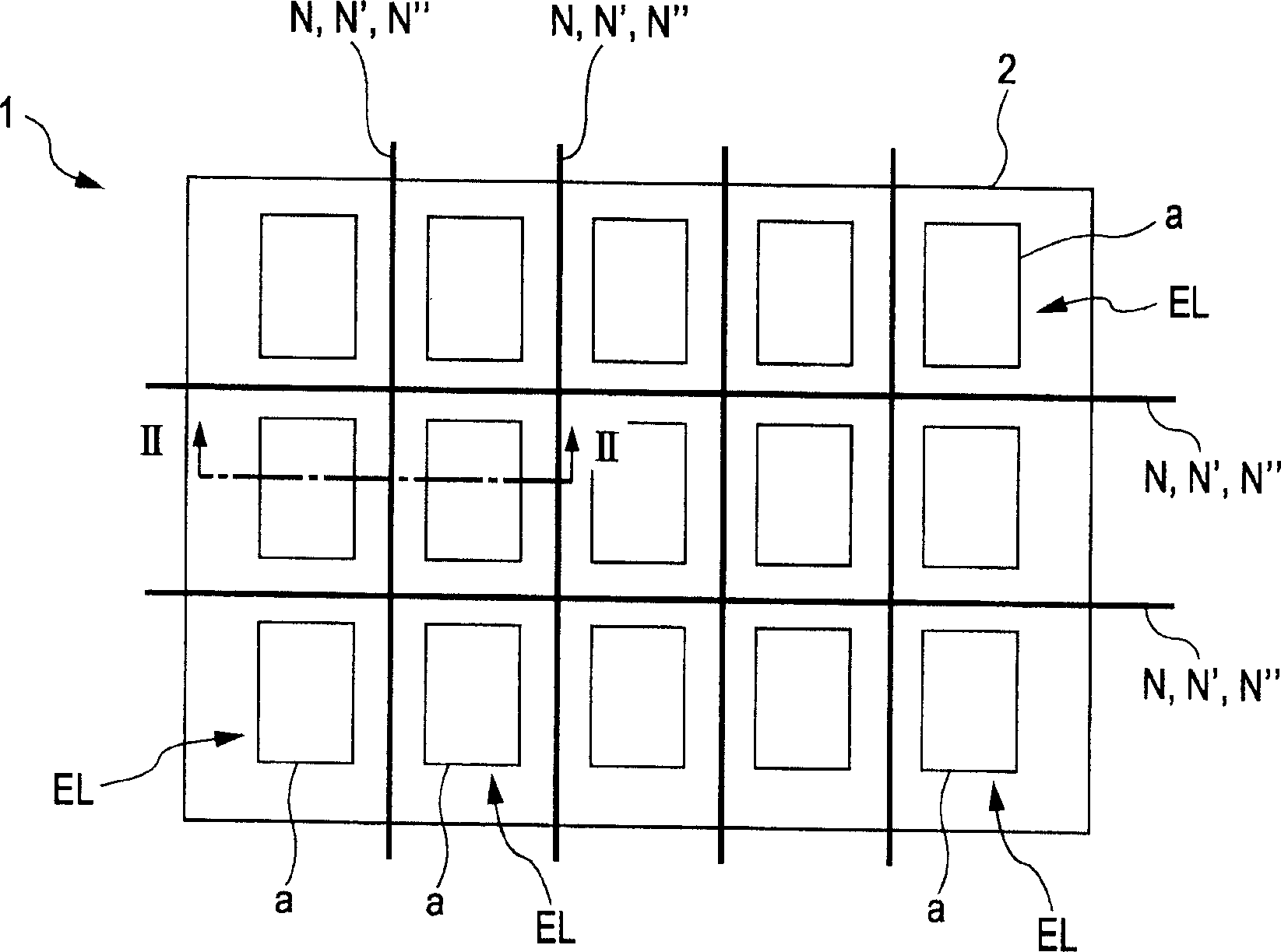
[0037] figure 1 It is a plan schematic diagram for explaining the structure of the display apparatus 1 of this 1st Embodiment. The display device 1 shown in this figure is an active matrix driven display device, and is formed by arranging a plurality of organic electroluminescence elements EL corresponding to each pixel a on a substrate 2 . In addition, between the pixels a-a, auxiliary wiring connected to the organic electroluminescent element EL is provided as follows.
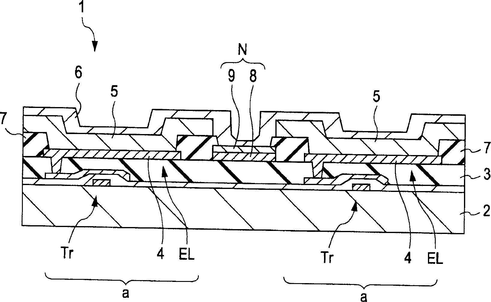
[0038] figure 2 is a schematic cross-sectional view for explaining the structure of the display device 1 according to the first embodiment, and corresponds to figure 1 The A-A' profile.
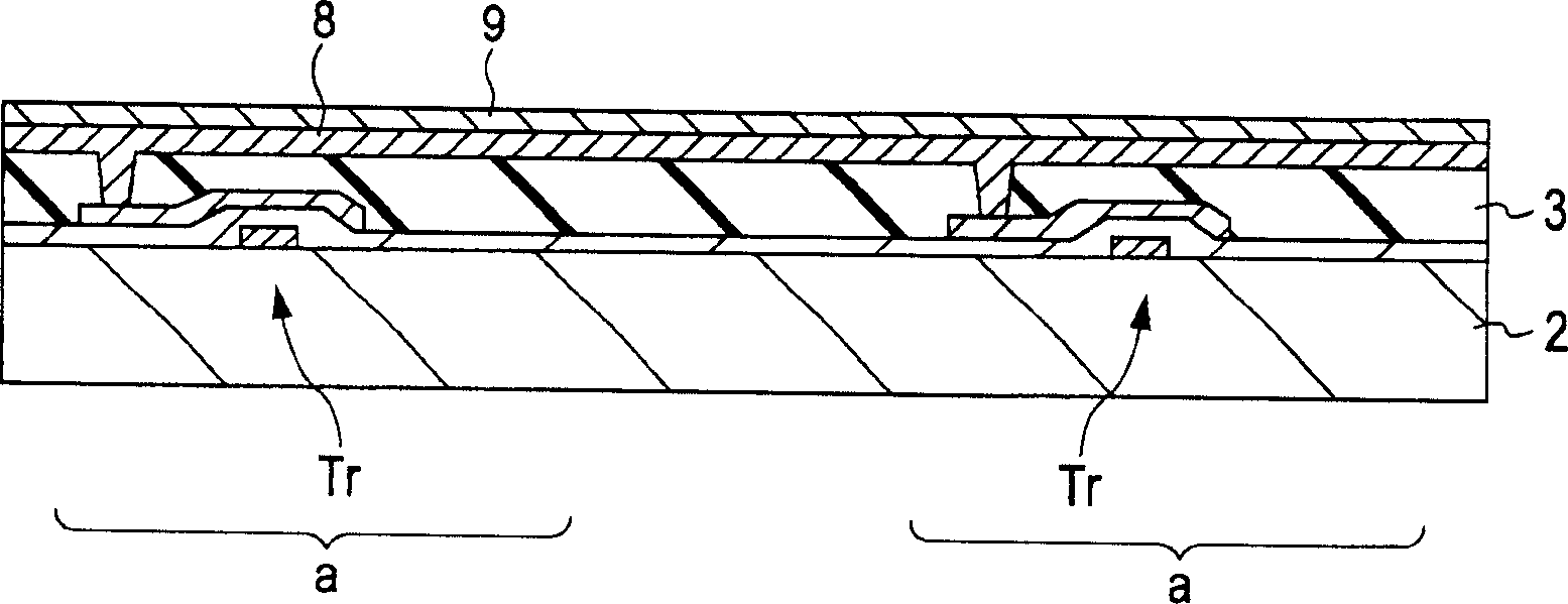
[0039] like figure 2 As shown, a pixel circuit including a thin film transistor Tr and a capacitive element not shown here is provided on a substrate 2 , and an interlayer insulating film 3 is provided in a state covering the pixel circuit. Simultaneously, on this interlayer insulating film 3, a structure for disposi...
no. 2 approach
[0069] FIG. 6 is a schematic cross-sectional view illustrating the configuration of a display device 1' shown in the second embodiment. The Figure 6 is equivalent to the previous figure 1 The A-A' profile. and Figure 6A The display device 1 ′ of the second embodiment shown is different from the display device 1 described in the first embodiment in the configuration of the auxiliary wiring N′, and the other configurations are the same.
[0070] That is, the auxiliary wiring N' on the display device 1' is composed only of a light absorbing layer made of a material that has a higher light absorption rate than the lower electrode 4 and has a higher light-to-heat conversion efficiency.
[0071] Furthermore, in the manufacture of the display device 1' constituted in this way, as Figure 6B As shown, the steps up to the formation of the interlayer insulating film 3 are performed in the same manner as in the first embodiment, and then the auxiliary wiring N' and the lower electrod...
no. 3 approach
[0075] Fig. 7 is a schematic cross-sectional view for explaining the structure of a display device 1" of the third embodiment. This Fig. 7 corresponds to the previous figure 1 The A-A' profile. and Figure 7A The display device 1 ″ of the third embodiment shown is different from the display device 1 described in the first embodiment in the structure of the auxiliary wiring N ″, and the other structures are the same.
[0076] That is, in the auxiliary wiring N" on the display device 1", the high conductive layer 8 made of the same material as the lower electrode 4 is provided on the upper layer of the light absorbing layer 9, and the light is exposed from the removed part of the high conductive layer 8. Structure of the absorbent layer 9 .
[0077] In the manufacture of the display device 1" thus constituted, as Figure 7B As shown, the steps up to the formation of the interlayer insulating film 3 are carried out in the same manner as in the previous first embodiment. After ...
PUM
 Abstract
Description
Claims
Application Information
 - R&D
- Intellectual Property
- Life Sciences
- Materials
- Tech Scout
- Unparalleled Data Quality
- Higher Quality Content
- 60% Fewer Hallucinations
Browse by: Latest US Patents, China's latest patents, Technical Efficacy Thesaurus, Application Domain, Technology Topic, Popular Technical Reports.
© 2025 PatSnap. All rights reserved.Legal|Privacy policy|Modern Slavery Act Transparency Statement|Sitemap|About US| Contact US: help@patsnap.com