Conveying chamber, substrate processing device, and substrate disorder detection method

A technology of a conveying device and a detection method, which is applied in the field of a conveying room, and can solve problems such as difficult detection and inability to apply position deviation detection of glass substrates

Inactive Publication Date: 2007-03-14
TOKYO ELECTRON LTD
View PDF1 Cites 12 Cited by
  • Summary
  • Abstract
  • Description
  • Claims
  • Application Information

AI Technical Summary

Problems solved by technology

[0007] The misalignment detection device of Patent Document 1 is aimed at small circular semiconductor wafers, and cannot be applied to misalignment detection of large rectangular glass substrates for FPDs.
In addition, the positional displacement detection device

Method used


Image

  • Conveying chamber, substrate processing device, and substrate disorder detection method
  • Conveying chamber, substrate processing device, and substrate disorder detection method
  • Conveying chamber, substrate processing device, and substrate disorder detection method

Examples


Embodiment Construction

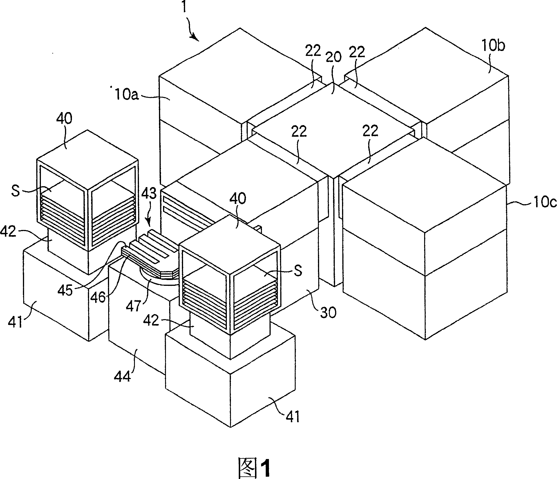
[0042] Next, preferred embodiments of the present invention will be described with reference to the drawings. Here, as a substrate processing apparatus, in a transfer chamber used in a multi-chamber plasma processing apparatus for performing plasma processing on a glass substrate for FPD (hereinafter simply referred to as a “substrate”) S, the substrate is abnormally treated. An example of detection will be described. Here, the FPD includes, for example, a liquid crystal display (LCD), a light emitting diode (LED) display, an electroluminescence (Electro Luminescence, EL) display, a fluorescent display tube (Vacuum Fluorescent Display, VFD), a plasma display panel (PDP), etc. .

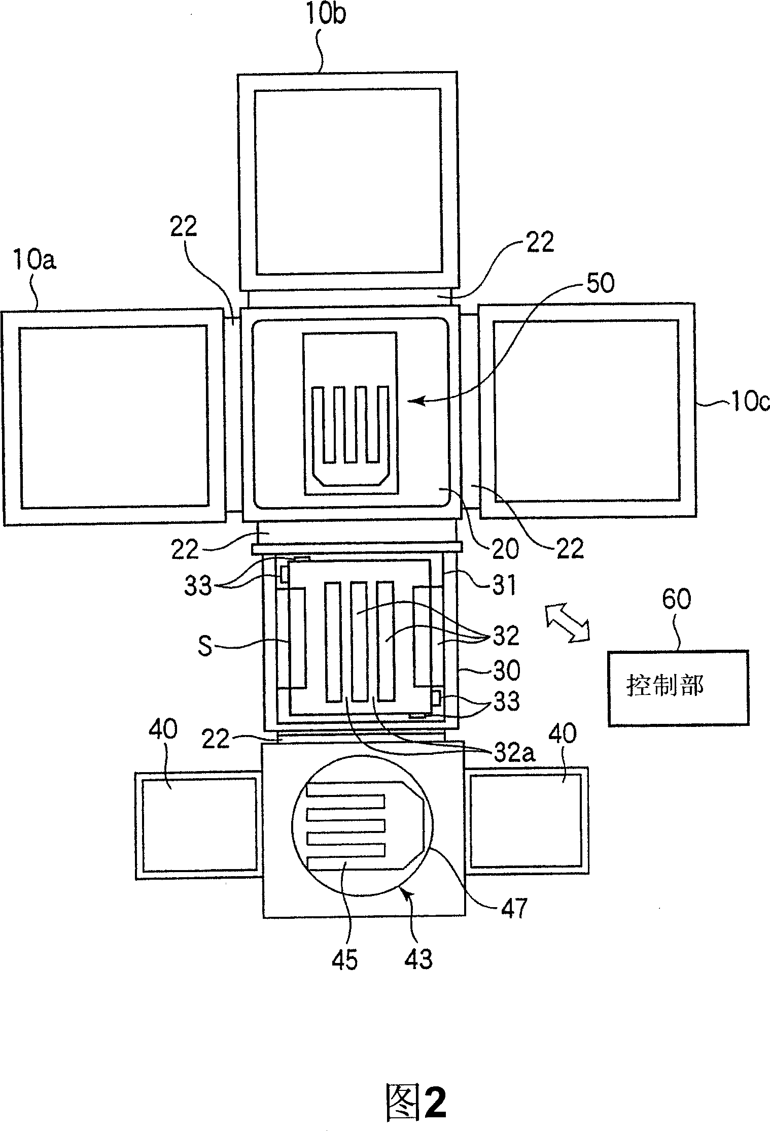
[0043] FIG. 1 is a perspective view schematically showing a plasma processing apparatus according to one embodiment of the substrate processing apparatus of the present invention, and FIG. 2 is a horizontal cross-sectional view schematically showing its interior.

[0044] In this vacuum processing a...


PUM


Abstract

The invention provides a substrate processing apparatus in which such a fault as misregistration or chipping of a large FPD substrate in a conveyance chamber can be detected certainly, and to provide a method for detecting the fault of the substrate. When a substrate (S) is mounted on the slide pick (513) of a conveying device and carried into a process chamber from the interior of a conveyance chamber (20) through a gate opening (22d), the substrate (S) is irradiated with light beams at the parts in the vicinity of the opposite ends shown by dashed lines (A, B) by means of a pair of sensors (70, 70) arranged on the right and left, and misregistration or defect of the substrate S is detected by its reflectivity or transmissivity.

Description

technical field [0001] The present invention relates to a transfer chamber, a substrate processing apparatus, and a substrate abnormality detection method, for example, to a transfer chamber of a substrate processing apparatus for performing etching or other processing on a glass substrate for a flat panel display (FPD), a substrate processing apparatus having the transfer chamber, And detection methods for substrate abnormalities such as substrate misalignment and chipping. Background technique [0002] In the manufacturing process of flat panel displays (FPDs) represented by liquid crystal displays (LCDs), a plurality of vacuum processing devices that perform predetermined processes such as etching, ashing, and film formation on glass substrates under vacuum are used. So-called multi-chamber type vacuum processing system. [0003] Such a vacuum processing system has a transfer chamber provided with a transfer device for transferring substrates, and a plurality of processi...

Claims


Application Information

Patent Timeline
IPC IPC(8): H01L21/677H01L21/67H01L21/66B65G49/06G01D5/34
CPCG02F1/1309H01L21/683
Inventor 冈部星儿末木英人
Owner TOKYO ELECTRON LTD
Why Eureka
Try Eureka