Method for repairing base plate of thin film transistor

A technology for repairing thin film transistors and substrates, which is applied in the field of repairing thin film transistor substrates, can solve problems such as increased manufacturing cost of thin film transistor substrates, and achieve the effect of saving costs

Inactive Publication Date: 2007-05-09
INNOCOM TECH SHENZHEN +1
View PDF0 Cites 5 Cited by
  • Summary
  • Abstract
  • Description
  • Claims
  • Application Information

AI Technical Summary

Problems solved by technology

[0006] In order to solve the above-mentioned problem of increasing the manufacturing cost of the thin film transistor substrate, it is necessary to provide a method for repairing the thin film transistor substrate with a lower cost

Method used


Image

  • Method for repairing base plate of thin film transistor
  • Method for repairing base plate of thin film transistor
  • Method for repairing base plate of thin film transistor

Examples


Embodiment Construction

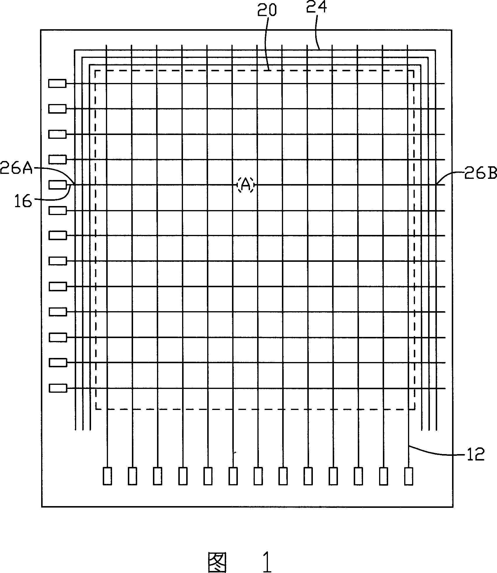
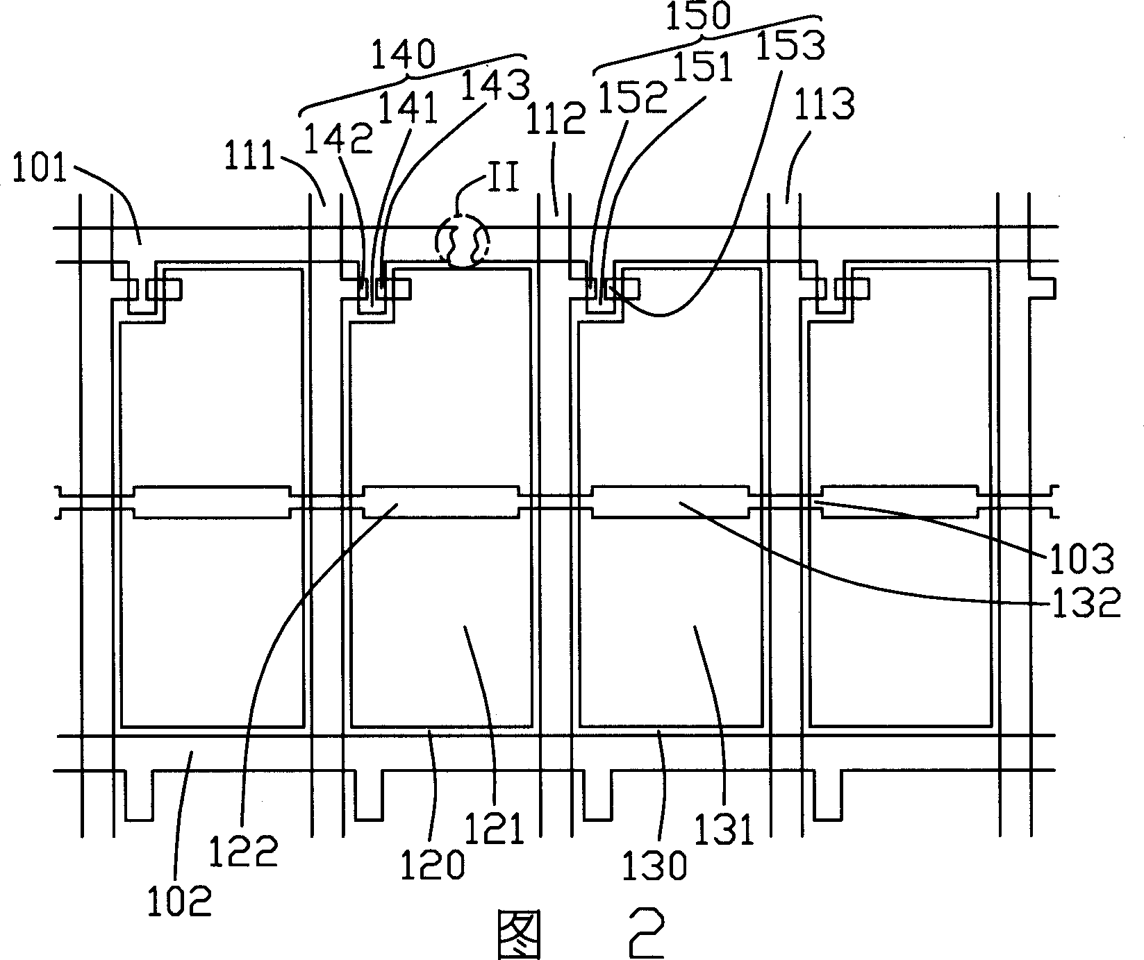
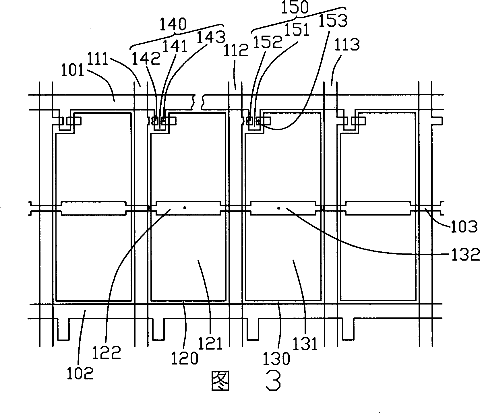
[0014] Please refer to FIG. 2 , which is a partial plan view of a TFT substrate with a gate line disconnected. The gate lines 101 and 102 perpendicularly cross the data lines 111 , 112 and 113 to define two pixel units 120 and 130 . The pixel unit 120 includes a pixel electrode 121 and a storage capacitor electrode 122 disposed below the pixel electrode 121 and forming a storage capacitor with the pixel electrode 121 . The pixel unit 130 includes a pixel electrode 131 and a storage capacitor electrode 132 disposed below the pixel electrode 131 and forming a storage capacitor with the pixel electrode 131 . The storage capacitor electrodes 122 , 132 and other storage capacitor electrodes in the same row are electrically connected through a connection line 103 . Two thin film transistors 140 and 150 are arranged at the corners of the two pixel units 120 and 130 respectively, the thin film transistor 140 includes a gate 141 electrically connected to the gate line 101 , a source 1...


PUM


Abstract

The invention is related to method for repairing base plate of thin film transistor (TFT). The base plate of TFT includes grid lines, data lines crossed to grid lines, pixel electrodes, and multiple TFT. Grid, source, and drain electrodes of TFT are connected to grid lines, data lines, and pixel electrodes electrically. A defect of electrical connection exists in a grid line. The repairing method includes following steps: cutting off electrical connection between source electrodes of two pieces of TFT located at two ends of the defect point and data line; connecting two pixel electrodes corresponding to the two pieces of TFT to the grid line electrically; connecting the two pixel electrodes electrically. The method can save cost.

Description

【Technical field】 [0001] The invention relates to a thin film transistor substrate repair method. 【Background technique】 [0002] At present, liquid crystal displays are gradually replacing traditional cathode ray tube (Cathode Ray Tube, CRT) displays used in calculators, and because liquid crystal displays are light, thin, and small, they are very suitable for desktop computers and personal computers. Digital Assistant (Personal Digital Assistant, PDA), portable phone, TV and various office automation and audio-visual equipment. The LCD panel is its main component. [0003] In the production process of liquid crystal panels, a large number of thin film transistors (Thin Film Transistor, TFT), pixel electrodes (Pixel Electrode) and multiple gates intersecting each other are often produced on the glass substrate through processes such as thin film deposition and lithography etching. Lines and data lines to form multiple pixel arrays (Pixel Array). However, during the entir...

Claims


Application Information

Patent Timeline
IPC IPC(8): H01L21/84H01L21/768G02F1/1362
Inventor 李庆华
Owner INNOCOM TECH SHENZHEN
Why Eureka
Try Eureka