Wafer fuse and its making method
A fuse and chip technology, which is applied in the manufacture of fuses, semiconductor/solid-state devices, emergency protection devices, etc., can solve the problems of increasing production costs, easy to pollute the environment, and cumbersome manufacturing processes, and achieve the effect of increasing production costs
- Summary
- Abstract
- Description
- Claims
- Application Information
AI Technical Summary
Problems solved by technology
Method used
Image

Examples
Embodiment Construction
[0015] Regarding the screw of the present invention, the technical means adopted and the effect of achieving the above-mentioned purpose are easy to understand. Hereby, a detailed description is made with the best embodiment in conjunction with the simple description of the drawings and the symbols of each component as follows:
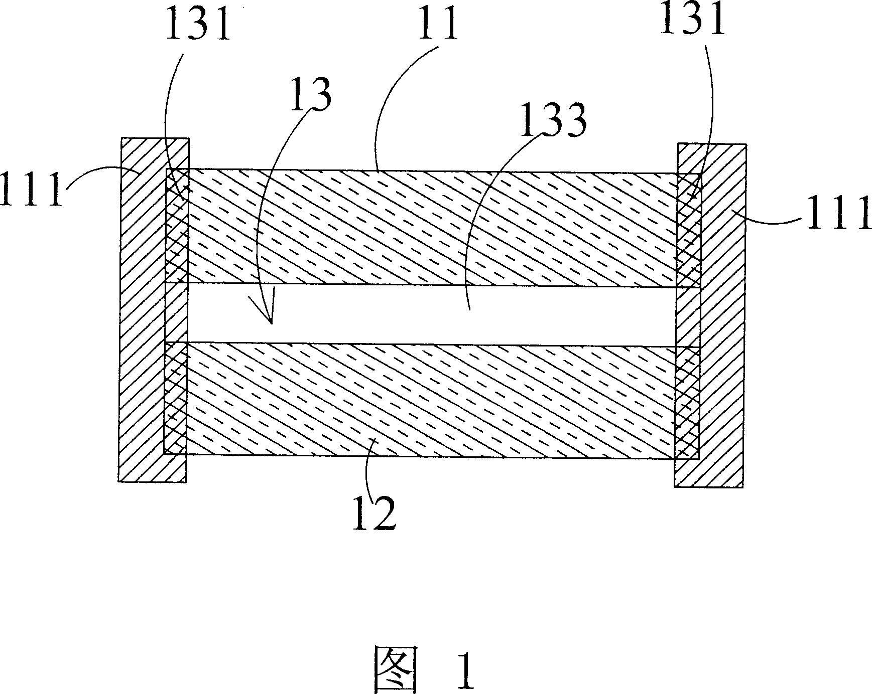
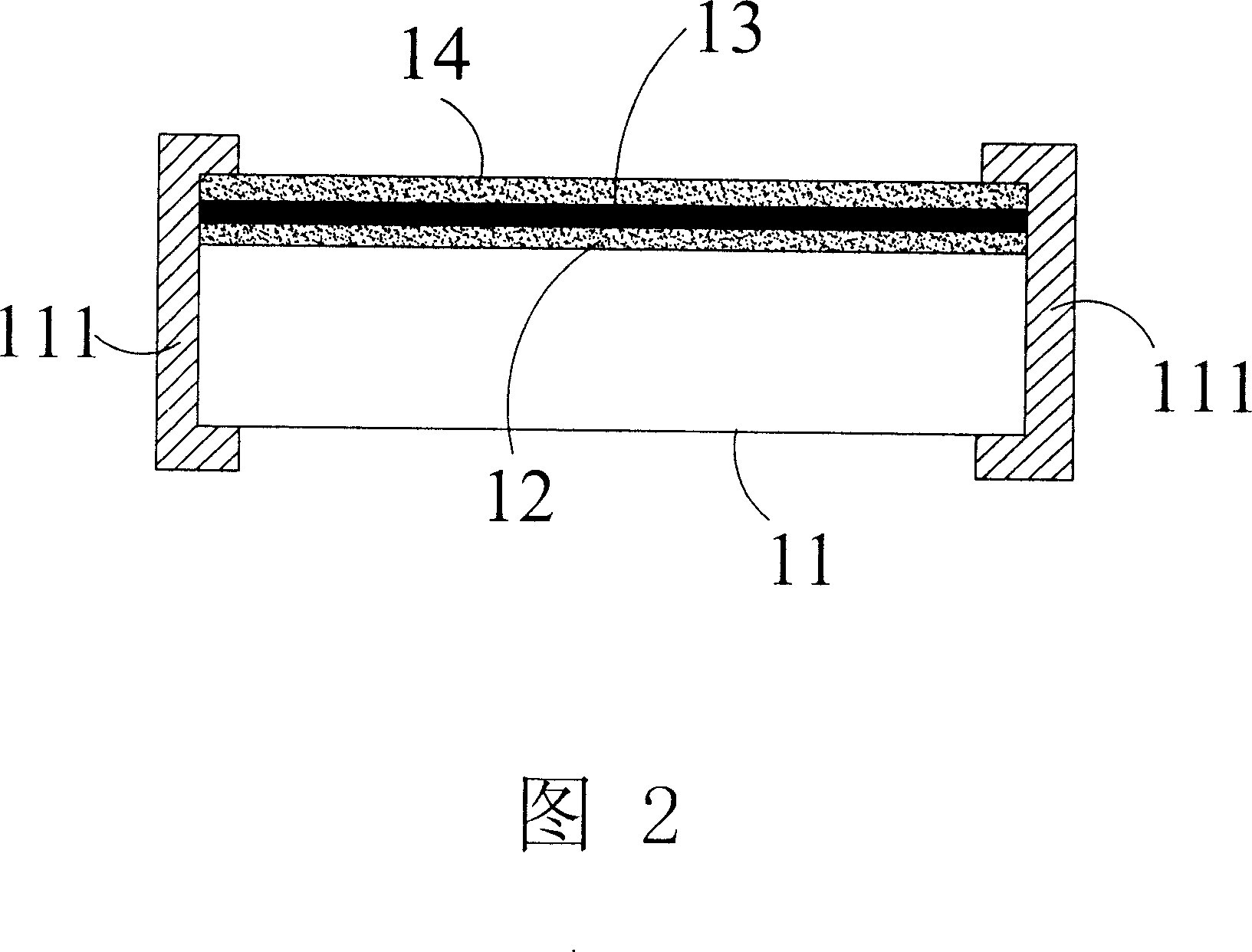
[0016] The present invention relates to a chip fuse and its manufacturing method, please refer to Figures 1 and 2, wherein the chip fuse includes:
[0017] Wafer substrate 11, forming terminal electrodes 111 on its two end faces;
[0018] The first matrix 12 is made by coating a layer of heat insulating material between the two terminal electrodes 111;
[0019] The second substrate 13 is made by printing an organic metal material on the surface of the first substrate 12 by a thick film printing method, and has two end parts 131 and a middle part 133, so that the two end parts 131 and the two ends The electrodes 111 are electrically connected;
[002...
PUM
 Abstract
Description
Claims
Application Information