Systems for displaying images

A technology of image display and liquid crystal display, which is applied in the field of thin film transistor liquid crystal display, and can solve problems such as peeling of reflective electrodes and affecting yield

Inactive Publication Date: 2007-06-13
TPO DISPLAY
View PDF0 Cites 1 Cited by
  • Summary
  • Abstract
  • Description
  • Claims
  • Application Information

AI Technical Summary

Problems solved by technology

As a result, problems such as peeling of reflecti

Method used


Image

  • Systems for displaying images
  • Systems for displaying images
  • Systems for displaying images

Examples


Embodiment Construction

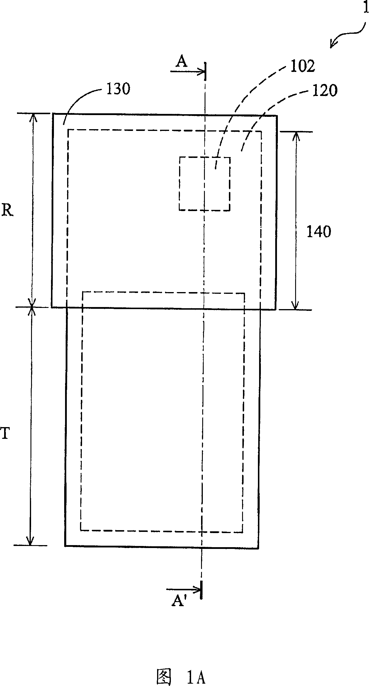
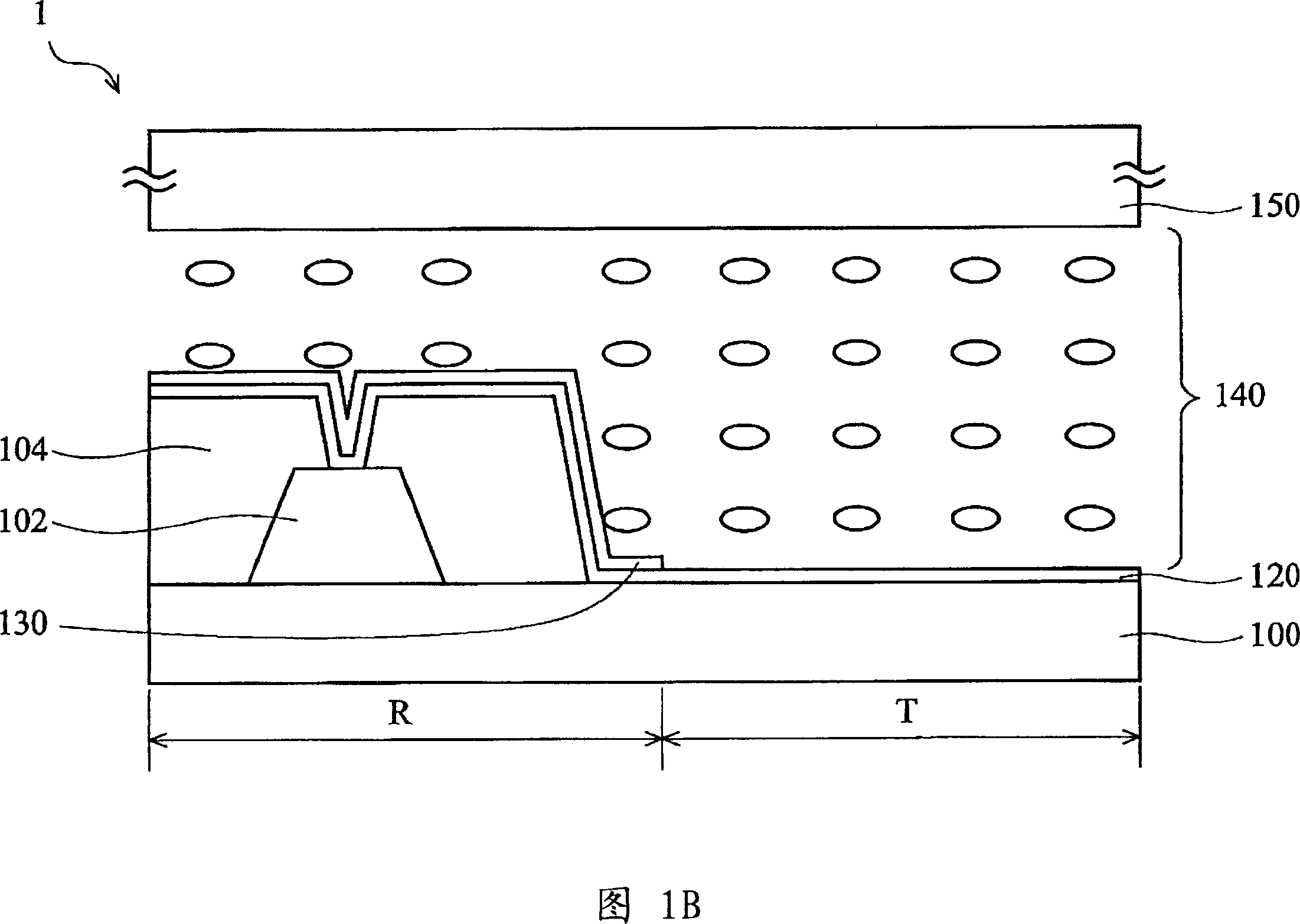
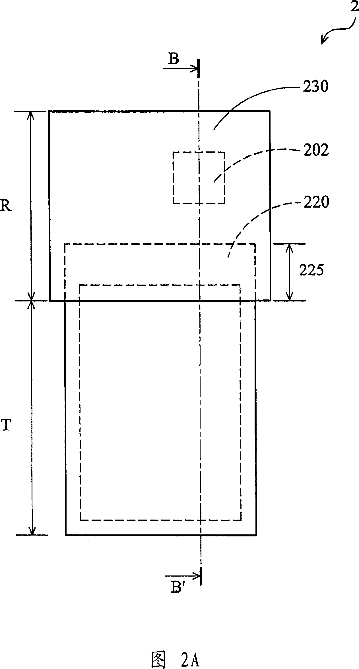
[0017] Several embodiments are provided below to illustrate the image display system and its manufacturing method of the present invention. In this regard, Figures 2A and 2B illustrate a preferred embodiment of the system. In particular, the system is coupled to a TFT-LCD panel 2, and the TFT-LCD panel 2 includes a first substrate, a second substrate, and a liquid crystal layer 240 disposed between the first substrate and the second substrate. Wherein, the first substrate is, for example, a color filter substrate 250 ; the second substrate is, for example, a TFT array substrate 200 on which a top-gate type TFT structure 202 is formed. Any sub-pixel of the thin film transistor array substrate 200 includes a reflective region R and a transmissive region T. The above-mentioned top-gate TFT structure 202 is covered by a flat layer 204 . The via window 260 transmits the planar layer 204 and part of the top gate TFT structure 202 to expose the source / drain of the top gate TFT stru...


PUM


Abstract

Systems for displaying images and methods of fabricating are provided. A representative system incorporates a transflective thin film transistor liquid crystal display (TFT-LCD) panel having a plurality of subpixels. The display panel comprises a first substrate with a transparent electrodeformed thereon, a reflective electrode on the transparent electrode, a second substrate opposite the first substrate, a liquid crystal layer between the first substrate and the second substrate. The panel also exhibits at least one of: the reflective electrode and the transparent electrode overlap by substantially between 100 and 1000 square micrometers; the reflective electrode and the transparent electrode overlap such that a ratio of an area of overlap of the reflective electrode and the transparent electrode to an area of a corresponding subpixel is substantially between 0.05 and 0.12; and a ratio of an area of the transparent electrode to an area of a corresponding subpixel is substantially between 0.5 and 0.6.

Description

technical field [0001] The invention relates to thin film transistor liquid crystal display technology. Background technique [0002] In the existing semi-transmissive and semi-reflective thin film transistor liquid crystal display technology, although the transparent electrode is completely covered by the reflective electrode, the adhesion may be deteriorated in subsequent processes. Regarding this problem, FIG. 1A is a partial top view showing a transflective and semi-reflective thin film transistor liquid crystal display panel 1 of a comparative example; Sectional view of line A-A'. [0003] As shown in FIGS. 1A and 1B , a color filter substrate 150, a processed thin film transistor array substrate 100 with a thin film transistor structure 102 formed thereon, and the processed thin film transistor array substrate 100 placed between the color filter substrate 150 and the above processed thin film transistor array substrate are provided. 100 between the liquid crystal lay...

Claims


Application Information

Patent Timeline
IPC IPC(8): G02F1/136G02F1/133H01L29/786
CPCG02F2203/01G02F1/134309G02F2203/02G02F1/133555
Inventor 陈志宏骆鸿毅陈政欣李俊谊陈威宏
Owner TPO DISPLAY
Why Eureka
Try Eureka