TFT-LCD (Thin Film Transistor Liquid Crystal Display) array base plate and manufacturing method thereof

A technology of array substrate and manufacturing method, which is applied in the field of TFT-LCD array substrate and its manufacturing, can solve the problems of small storage capacitance and influence on display quality, achieve the effect of increasing size, improving display quality, and wide application prospects

Inactive Publication Date: 2010-11-17
BOE TECH GRP CO LTD +1
View PDF0 Cites 37 Cited by
  • Summary
  • Abstract
  • Description
  • Claims
  • Application Information

AI Technical Summary

Problems solved by technology

[0005] The object of the present invention is to provide a TFT-LCD array substrate and its manufacturing method, which can effectively solve the problem

Method used


Image

  • TFT-LCD (Thin Film Transistor Liquid Crystal Display) array base plate and manufacturing method thereof
  • TFT-LCD (Thin Film Transistor Liquid Crystal Display) array base plate and manufacturing method thereof
  • TFT-LCD (Thin Film Transistor Liquid Crystal Display) array base plate and manufacturing method thereof

Examples


Embodiment Construction

[0060] The technical solutions of the present invention will be described in further detail below with reference to the accompanying drawings and embodiments.

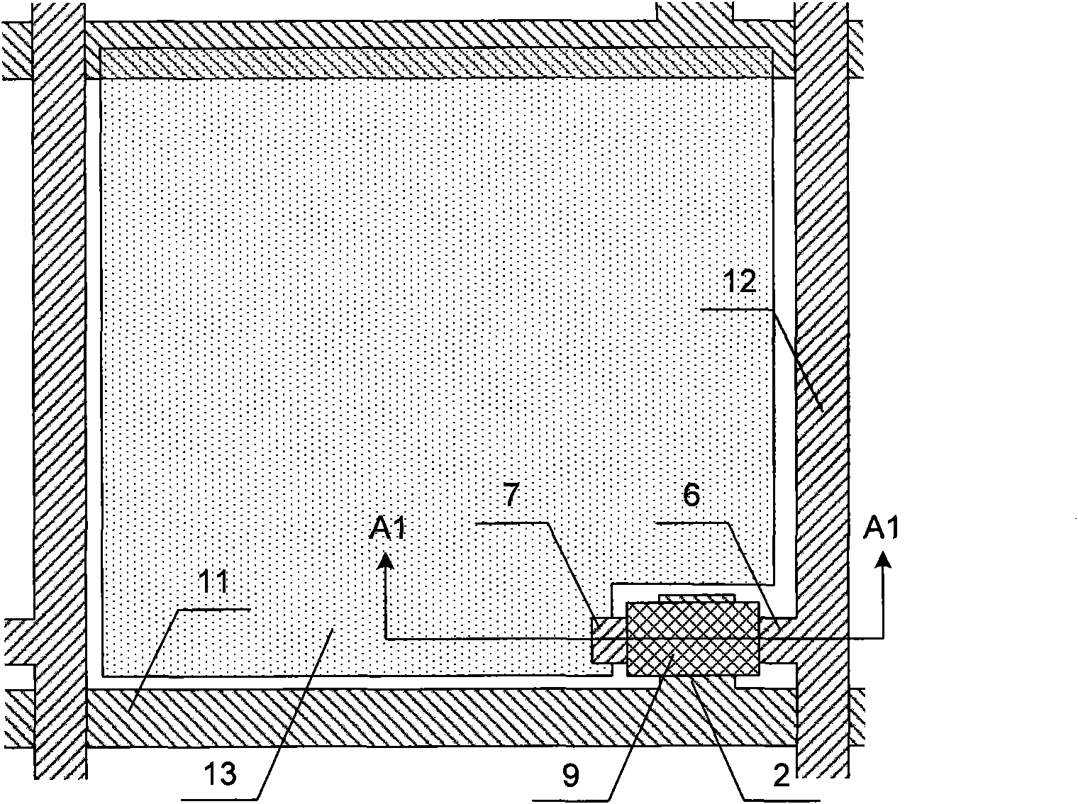
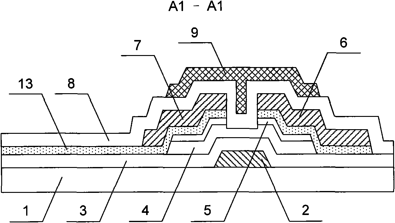
[0061] figure 1 It is a plan view of the first embodiment of the TFT-LCD array substrate of the present invention, reflecting the structure of a pixel unit, figure 2 for figure 1 Sectional view of A1-A1 in the middle. Such as figure 1 with figure 2 As shown, the main structure of the TFT-LCD array substrate in this embodiment includes gate lines 11, data lines 12, pixel electrodes 13 and thin film transistors, the gate lines 11 and data lines 12 perpendicular to each other define pixel regions, and the thin film transistors and pixel electrodes 13 is formed in the pixel area, the gate line 11 is used to provide the turn-on signal to the thin film transistor, and the data line 12 is used to provide the data signal to the pixel electrode 13 . Specifically, the TFT-LCD array substrate of this embodiment includes ga...


PUM


Abstract

The invention relates to a TFT-LCD (Thin Film Transistor Liquid Crystal Display) array base plate and a manufacturing method thereof. The array base plate comprises a grid line and a data line, wherein a pixel electrode and a thin film transistor are formed in a pixel region limited by the grid line and the data line, and a shielding layer is formed above a TFT channel region of the thin film transistor. The manufacturing method comprises the following steps of: depositing a grid metal thin film to form the figures of the grid line and a grid electrode; depositing a grid insulating layer, a semiconductor thin film and a doped semiconductor thin film to form the figure of an active layer; depositing a transparent conductive thin film and a source and drain metal thin film to form the figures of a pixel electrode, the data line, a source electrode, a drain electrode and the TFT channel region; and depositing a passivation layer and a shielding thin film to form the figures of the shielding layer, a grid line interface through hole and a data line interface through hole, wherein the shielding layer is positioned above the TFT channel region. The invention avoids the generation of leakage current under the condition of not increasing a production process and improves the size of capacitance storage in unit area.

Description

technical field [0001] The invention relates to a liquid crystal display and a manufacturing method thereof, in particular to a TFT-LCD array substrate and a manufacturing method thereof. Background technique [0002] Thin Film Transistor Liquid Crystal Display (TFT-LCD for short) has the characteristics of small size, low power consumption, and no radiation. It has developed rapidly in recent years and occupies a dominant position in the current flat panel display market. The liquid crystal panel is one of the most important components in TFT-LCD, mainly including the array substrate and the color filter substrate that are boxed together and the liquid crystal is sandwiched between them. At present, the manufacture of array substrates is completed through a group of patterning processes to form structural graphics. One patterning process forms a layer of structural graphics. For TFT-LCD, the TFT-LCD array substrate and manufacturing process determine its product performance...

Claims


Application Information

Patent Timeline
IPC IPC(8): H01L27/12H01L29/786H01L29/10H01L21/84H01L21/768H01L21/027G02F1/1362
CPCH01L27/1214G02F2001/136236H01L29/78633G02F1/1362H01L27/1288H01L29/66765H01L27/12H01L27/156H01L27/124G02F1/136236
Inventor 刘翔
Owner BOE TECH GRP CO LTD
Why Eureka
Try Eureka