FFS (Fringe Field Switching) type TFT-LCD (Thin Film Transistor Liquid Crystal Display) array substrate and manufacturing method thereof

A manufacturing method and array substrate technology, which are applied in semiconductor/solid-state device manufacturing, optics, instruments, etc., can solve the problems of widening TFT channel, excessive etching of TFT channel, and difficulty in controlling the degree of etching, so as to save costs. , The effect of improving yield and performance

Active Publication Date: 2011-01-26
BOE TECH GRP CO LTD +1
View PDF3 Cites 34 Cited by
  • Summary
  • Abstract
  • Description
  • Claims
  • Application Information

AI Technical Summary

Problems solved by technology

Since it is difficult to control the degree of etching by wet etching, the problem of over etching of the TFT channel (Over Etch) is inevitable.
For the significant TFT channel in the array su

Method used


Image

  • FFS (Fringe Field Switching) type TFT-LCD (Thin Film Transistor Liquid Crystal Display) array substrate and manufacturing method thereof
  • FFS (Fringe Field Switching) type TFT-LCD (Thin Film Transistor Liquid Crystal Display) array substrate and manufacturing method thereof
  • FFS (Fringe Field Switching) type TFT-LCD (Thin Film Transistor Liquid Crystal Display) array substrate and manufacturing method thereof

Examples


Embodiment Construction

[0060] It should be noted:

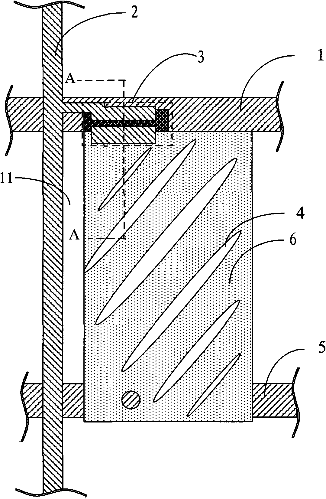
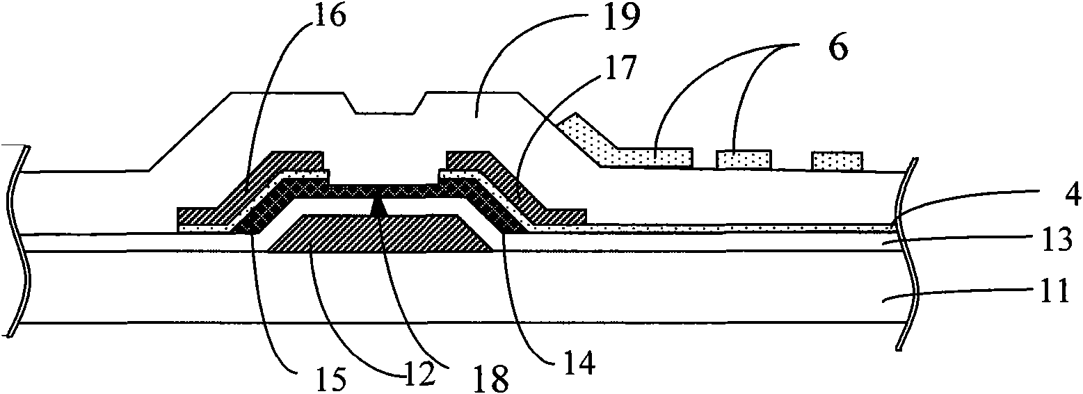
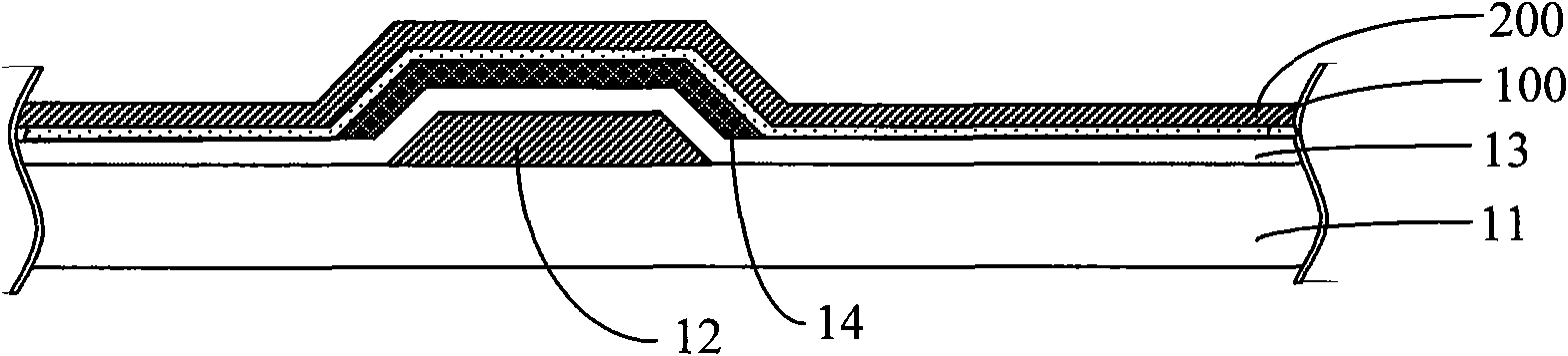
[0061] 1. The "upper" in "X is arranged on Y" or "X is arranged on Y" in the present invention includes the meaning that X is in contact with Y, and X is located above Y. In the present invention, as attached As shown in the figure, the transparent substrate is defined as being set at the bottom;

[0062] 2. The patterning process referred to in the present invention includes processes such as photoresist coating, masking, exposure, development, etching, photoresist stripping, and the photoresist is an example of a positive photoresist;

[0063] 3. The "so-and-so area" mentioned in the present invention is the area where a certain figure is mapped on the transparent substrate, that is, the area has the same shape as the certain figure, such as the grid line area, that is, the figure of the grid line is in the transparent substrate. The mapped area on the substrate can also be understood as the area on the transparent substrate where the grid patte...


PUM


Abstract

The invention discloses an FFS (Fringe Field Switching) type TFT-LCD (Thin Film Transistor Liquid Crystal Display) array substrate and a manufacturing method thereof. The method comprises the following steps of: depositing a first metal film on a transparent substrate, and forming a pattern comprising a grid line, a grid electrode and a common electrode line through a first pattern composition process; depositing a grid insulating layer, an active layer film and a second metal film, and retaining the active layer film and the second metal film in a data line region, a source electrode region,a drain electrode region and a TFT channel region through a second pattern composition process; depositing a first transparent conducting film, and forming a pattern comprising a source electrode, a drain electrode, a TFT channel and a pixel electrode through a third pattern composition process; and depositing a passivation layer, forming a pattern comprising a connecting hole through a fourth pattern composition process, carrying out photoresist ashing process, depositing a second transparent conducting layer, and forming a pattern comprising a common electrode through an off-ground stripping process. The invention can reduce the excessive etching degree of the TFT channel and can ensure the display performance of a liquid crystal display.

Description

technical field [0001] The invention relates to a liquid crystal display, in particular to an FFS type TFT-LCD array substrate capable of reducing the degree of excessive etching of a TFT channel and a manufacturing method thereof. Background technique [0002] Thin Film Transistor Liquid Crystal Display (TFT-LCD for short) is a main flat panel display (Flat Panel Display, FPD for short). [0003] According to the direction of the electric field driving the liquid crystal, the TFT-LCD is divided into a vertical electric field type and a horizontal electric field type. Among them, the vertical electric field TFT-LCD needs to form pixel electrodes on the array substrate and the common electrode on the color filter substrate; however, the horizontal electric field TFT-LCD needs to form the pixel electrodes and common electrodes on the array substrate at the same time. Therefore, when manufacturing the array substrate of the horizontal electric field type TFT-LCD, it is necessa...

Claims


Application Information

Patent Timeline
IPC IPC(8): G02F1/1362G02F1/1368H01L21/82
CPCH01L27/1214H01L27/1288G02F2001/134372G02F1/134363G02F1/134372
Inventor 崔承镇宋泳锡刘圣烈
Owner BOE TECH GRP CO LTD
Why Eureka
Try Eureka