Pvd aln film with oxygen doping for a low etch rate hardmask film

Active Publication Date: 2013-11-07
APPLIED MATERIALS INC
View PDF5 Cites 3 Cited by
  • Summary
  • Abstract
  • Description
  • Claims
  • Application Information

AI Technical Summary

Benefits of technology

[0010]The present invention generally relates to a doped aluminum nitride hardmask and a method of making a doped aluminum nitride hardmask. By adding a small amount of dopant, such as oxygen, when forming the aluminum nitride hardmask, the wet etch rate of the hardmask can be significantly reduce

Problems solved by technology

It has become increasingly more difficult to not only shrink the size of the semiconductor chip, but additionally, the individual features that form the electrical

Method used


Image

  • Pvd aln film with oxygen doping for a low etch rate hardmask film
  • Pvd aln film with oxygen doping for a low etch rate hardmask film
  • Pvd aln film with oxygen doping for a low etch rate hardmask film

Examples


Embodiment Construction

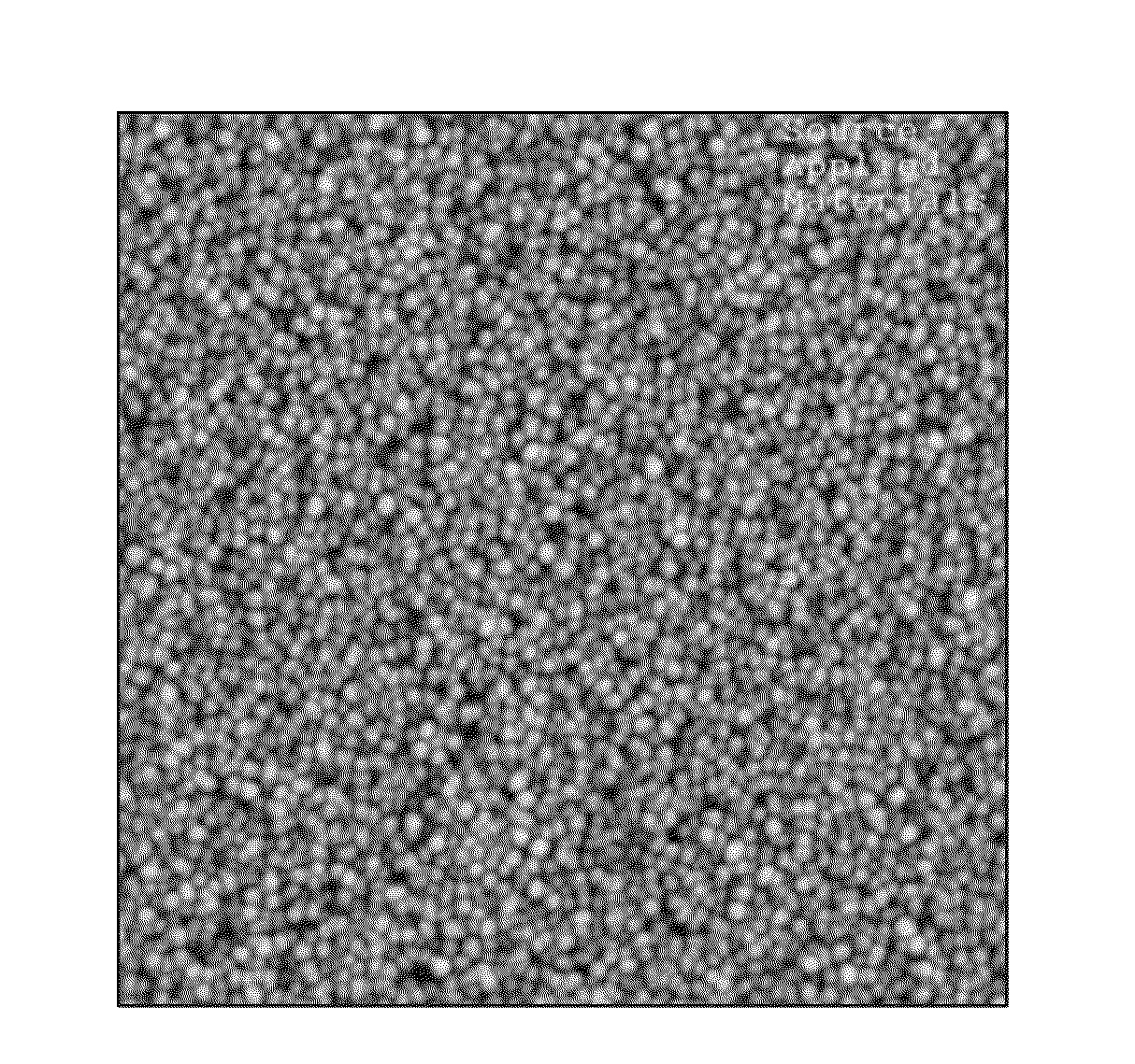
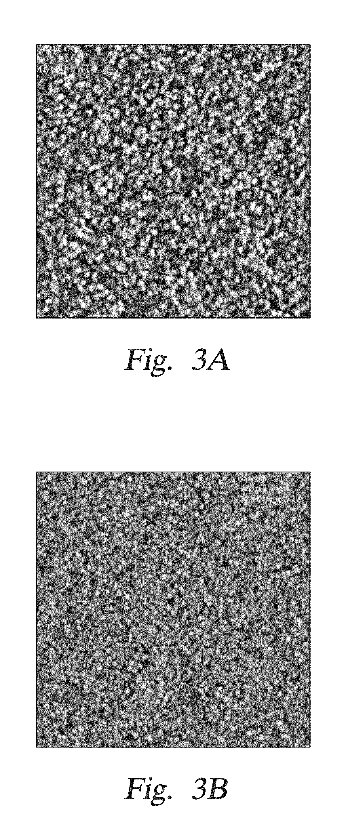
[0018]The present invention generally relates to a doped aluminum nitride hardmask and a method of making a doped aluminum nitride hardmask. By adding a small amount of dopant, such as oxygen, when forming the aluminum nitride hardmask, the wet etch rate of the hardmask can be significantly reduced. Additionally, due to the presence of the dopant, the grain size of the hardmask is reduced compared to a non-doped aluminum nitride hardmask. The reduced grain size leads to smoother features in the hardmask which leads to more precise etching of the underlying layer when utilizing the hardmask.

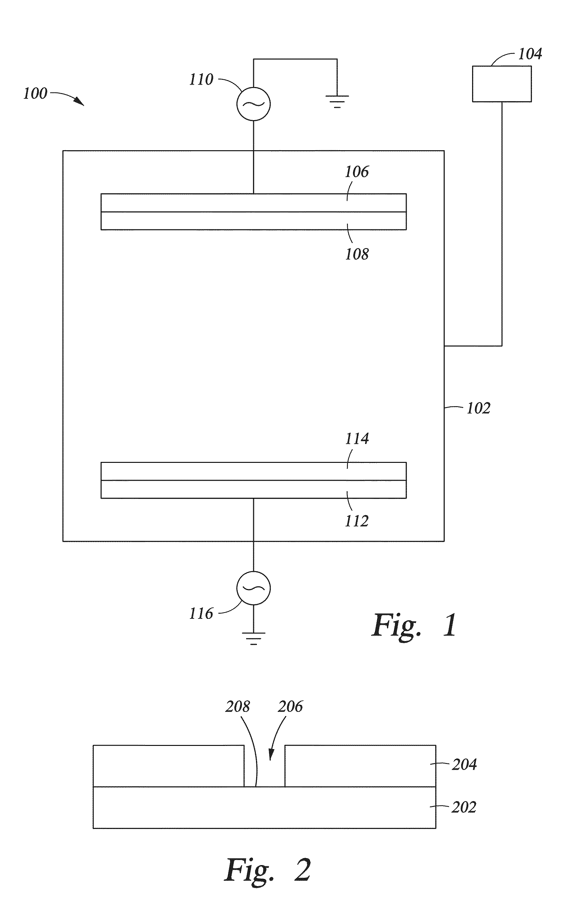
[0019]FIG. 1 is a schematic cross sectional illustration of a PVD apparatus 100 according to one embodiment. The apparatus 100 includes a chamber body 102. Gas is delivered to the chamber body 102 from a gas source 104. A sputtering target 108 is disposed within the chamber body 102 opposite a substrate 114. The sputtering target 108 is bonded to a backing plate 106. A bias is applied to the backi...


PUM

PropertyMeasurementUnit
Temperatureaaaaaaaaaa
Pressureaaaaaaaaaa

Abstract

The present invention generally relates to a doped aluminum nitride hardmask and a method of making a doped aluminum nitride hardmask. By adding a small amount of dopant, such as oxygen, when forming the aluminum nitride hardmask, the wet etch rate of the hardmask can be significantly reduced. Additionally, due to the presence of the dopant, the grain size of the hardmask is reduced compared to a non-doped aluminum nitride hardmask. The reduced grain size leads to smoother features in the hardmask which leads to more precise etching of the underlying layer when utilizing the hardmask.

Description

CROSS-REFERENCE TO RELATED APPLICATIONS[0001]This application claims benefit of U.S. Provisional Patent Application Ser. No. 61 / 637,804 (APPM / 17436L), filed Apr. 24, 2012, which is herein incorporated by reference.BACKGROUND OF THE INVENTION[0002]1. Field of the Invention[0003]Embodiments of the present invention generally relate to a doped aluminum nitride hardmask and a method of making a doped aluminum nitride hardmask.[0004]2. Description of the Related Art[0005]As semiconductor devices continue to shrink in size, the precision needed to form such small devices increases. It has become increasingly more difficult to not only shrink the size of the semiconductor chip, but additionally, the individual features that form the electrical interconnects.[0006]There are numerous processes that are performed to fabricate a semiconductor chip. Patterning is one of those processes. In a patterning process, a mask, such as a hardmask, is formed over one or more layers to be patterned. There...

Claims


Application Information

Patent Timeline
IPC IPC(8): C04B35/581C23C14/06
CPCC04B35/581C23C14/0617H01L21/0332H01L21/32139H01L21/02631H01L21/0254H01L21/02573H01L21/02178H01L21/02266
Inventor CAO, YONGDAITO, KAZUYAJAKKARAJU, RAJKUMARTANG, XIANMIN
Owner APPLIED MATERIALS INC
Why Eureka
Try Eureka