Manufacture method for flip-chip and bare chip assembly

A manufacturing method and bare chip technology, applied in the direction of electrical components, electrical solid devices, semiconductor devices, etc., to achieve the effect of mitigating potential damage, precise electroplating position, and strengthening protection

Inactive Publication Date: 2017-09-26
LEADCORE TECH +1
View PDF6 Cites 2 Cited by
  • Summary
  • Abstract
  • Description
  • Claims
  • Application Information

AI Technical Summary

Problems solved by technology

[0005] It is not difficult to see that in the prior art, the PI layer covered on the surface of the chip mainly exists as a stress buffer layer for the copper pillars, and as the diameter of the copper pillars gradually shrinks, the influence of the tangential stress on the strength of the copper pillars becomes increasingly prominent. This brings about related issues such as packaging yield and reliability.

Method used


Image

  • Manufacture method for flip-chip and bare chip assembly
  • Manufacture method for flip-chip and bare chip assembly
  • Manufacture method for flip-chip and bare chip assembly

Examples


Embodiment Construction

[0020] In order to make the object, technical solution and advantages of the present invention clearer, various embodiments of the present invention will be described in detail below in conjunction with the accompanying drawings. However, those of ordinary skill in the art can understand that, in each implementation manner of the present invention, many technical details are provided for readers to better understand the present application. However, even without these technical details and various changes and modifications based on the following implementation modes, the technical solution claimed in each claim of the present application can be realized.

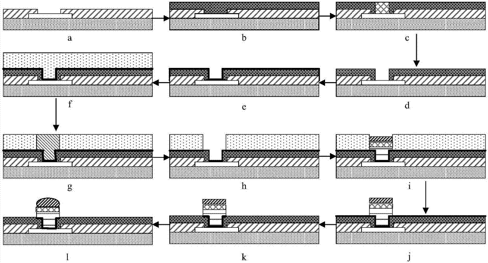
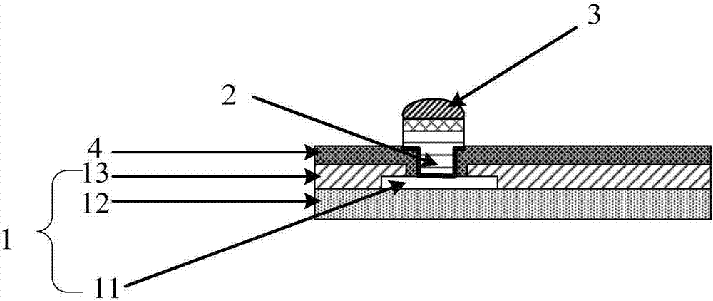
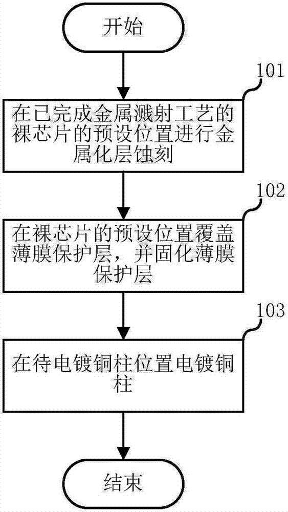
[0021] The first embodiment of the present invention relates to a flow chart of a method for manufacturing a flip chip, the specific process is as follows image 3 shown. In this embodiment, for ease of understanding, it is also combined with Figure 4(a) to Figure 4(m) The structural schematic diagrams of the bare chip co...


PUM


Abstract

The invention relates to the semiconductor field and discloses a manufacture method for a flip-chip and a bare chip assembly. The manufacture method comprises steps of performing metallization layer etching on a preset position of a bare chip on which metal spurting technology is finished, wherein the preset position is an area beyond a position of a copper column to be electroplated on the bare chip, covering a film protection layer in the preset position of the bare chip and hardening the film protection layer, and electroplating the copper column in the position of the copper column to be electroplated. Through the arrangement, the manufacture method and the bare chip assembly add an extra protection layer on the bare chip in the prior art, which effectively alleviates a potential damage on the copper column which is caused by a tangential stress around the copper column, enhances protection on the flip-chip copper column protection and improves packaging yield rate and reliability.

Description

technical field [0001] The invention relates to the field of semiconductors, in particular to chip packaging technology. Background technique [0002] The Flip chip packaging process is a hot spot in the field of semiconductor packaging today. Compared with the traditional wire-bonding packaging process, the Flip chip packaging process faces the active area of ​​the bare chip to the substrate. Solder bumps (solder balls and copper pillars) arranged in an array on the chip realize the interconnection between the bare chip and the substrate. The bare chip is directly mounted on the substrate in an inverted manner, which greatly shortens the interconnection length, and has small RC delay and heat dissipation. Good performance, high IO density, small package area, and thin thickness are very suitable for the current development direction of IC products with high speed, high performance, high IO density, and miniaturization. However, in the current mainstream Flip chip packaging...

Claims


Application Information

Patent Timeline
Patent Type & Authority Applications(China)
IPC IPC(8): H01L21/56H01L21/60H01L23/31
CPCH01L21/563H01L23/3171H01L24/81
Inventor 周涛王沛王强
Owner LEADCORE TECH
Why Eureka
Try Eureka