Preparation method of semiconductor structure

A semiconductor and gate structure technology, applied in the field of semiconductor structure preparation, can solve the problems of low yield of high-voltage transistors, exposure, photoresist peeling, etc.

Active Publication Date: 2021-08-20
江苏茂硕新材料科技有限公司
View PDF4 Cites 1 Cited by
  • Summary
  • Abstract
  • Description
  • Claims
  • Application Information

AI Technical Summary

Problems solved by technology

High-voltage transistors need to form silicide layers on the source, drain, and gate to reduce contact resistance. In order to realize this device structure, photoresist is needed to define the drift region, and one side of the photoresist will fall on the gate. On the pole side wall, when exposed, scattered light is likely to be reflected by the side wall, causing the bottom of the photoresist to be exposed, resulting in peeling off of the photoresist, which will cause the problem of low yield of high-voltage transistors

Method used


Image

  • Preparation method of semiconductor structure
  • Preparation method of semiconductor structure
  • Preparation method of semiconductor structure

Examples


Embodiment 1

[0053] In this embodiment, a method for preparing a semiconductor structure is proposed, the semiconductor structure is a high-voltage transistor, and the method for preparing the semiconductor structure includes the following steps:

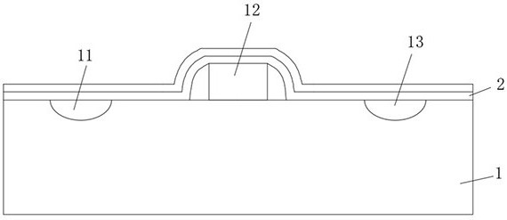
[0054] S1: reference figure 2 , providing a substrate 1, an active region 11 and a drain region 13 are formed in the substrate 1, a gate structure 12 is formed between the source region 11 and the drain region 13, and a gate structure 12 is formed between the source region 11 and the drain region 13. There is a drift region between them, and a dielectric layer 2 is formed on the substrate 1, and the dielectric layer 2 covers the gate structure 12, the source region 11, the drain region 13 and the drift region;

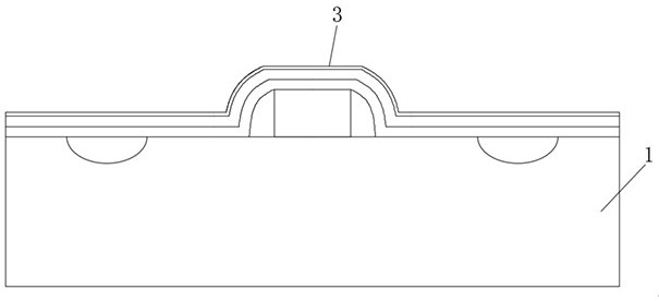
[0055] S2: Reference image 3 , forming an anti-reflection layer 3 on the dielectric layer 2 by vapor deposition;

[0056] S3: Reference Figure 4 and Figure 5 , form A photoresist layer 4 on anti-reflection layer 3, and A photores...

Embodiment 2

[0063] refer to Figure 8 , in this embodiment, a processing device for semiconductor structure preparation is proposed, including a fixed shaft 400, a clamping mechanism 200 and a loading tray 100, the fixed shaft 400 is vertically arranged, and the clamping mechanisms 200 are distributed in a circular array around the fixed shaft 400 , the clamping mechanism 200 is used to clamp the loading tray 100, the loading tray 100 is loaded with components, and the side of the fixed shaft 400 is provided with processing stations, the number of processing stations is the same as that of the clamping mechanism 200 and the positions correspond to each other, the fixed shaft 400 An adjustment mechanism is installed on the top, and the adjustment mechanism is used to adjust the clamping mechanism 200 to intermittently enter and exit each station sequentially. Through the above arrangement, it is possible to adjust the clamping mechanism 200 to move in and out of each station intermittently...


PUM


Abstract

The invention relates to the field of preparation of semiconductor elements, and particularly discloses a preparation method of a semiconductor structure, which comprises the following steps: firstly, forming a dielectric layer on a substrate, forming a reflection-resistant layer on the dielectric layer, forming an A photoresist layer on the reflection-resistant layer, and exposing and developing the A photoresist layer. Under the effect of thereflection-resistant layer, the arc-shaped part of the dielectric layer at the gate structure does not reflect light, so that the problem that the patterned photoresist layer generates defects and is even stripped off is avoided, then the opening is etched, the reflection-resistant layer is removed, and finally the silicide layer is formed. the processing device is adopted to remove the anti-reflection layer, the processing device comprises a fixing shaft, a clamping mechanism, a loading tray and an adjusting mechanism, the clamping mechanism is used for clamping the loading tray, elements are loaded in the loading tray, and the adjusting mechanism is used for adjusting the clamping mechanism to intermittently and sequentially enter and exit from a dissolving tank, a flushing tank and a drying mechanism. The reflection-resistant layer layer on the element is dissolved, washed and dried, and automatic machining is achieved.

Description

technical field [0001] The invention relates to the field of semiconductor element preparation, in particular to a method for preparing a semiconductor structure. Background technique [0002] At present, high-voltage transistors are widely used in integrated high-voltage power management circuits of various industrial electronic equipment and consumer electronic equipment, or in memory read and write circuits. Usually, the input voltage of high-voltage transistors is relatively high (5V ~ 600V). Therefore, when high-voltage transistors are used as When the power transistor is applied, it should have a higher breakdown voltage (breakdown voltage) to improve the stability of the work. In order to achieve a higher breakdown voltage, a longer drift area (drift area, formed between the gate and Source or gate and drain) to withstand high voltage, no metal silicide can be formed on the drift region. High-voltage transistors need to form silicide layers on the source, drain, and ...

Claims


Application Information

Patent Timeline
Patent Type & Authority Applications(China)
IPC IPC(8): H01L21/336H01L21/027H01L21/311H01L21/67
CPCH01L21/0274H01L21/31144H01L21/67167H01L29/66681
Inventor 杨崇秋吉成东周林
Owner 江苏茂硕新材料科技有限公司
Why Eureka
Try Eureka