Array substrate and display device

An array substrate, column pixel technology, applied in static indicators, instruments, semiconductor devices, etc., can solve problems such as hindering the development of large-size and thin-frame LCDs, and achieve the effect of balancing unbalanced effects and narrowing the frame.

Inactive Publication Date: 2012-08-08
BOE TECH GRP CO LTD +1
View PDF5 Cites 35 Cited by
  • Summary
  • Abstract
  • Description
  • Claims
  • Application Information

AI Technical Summary

Problems solved by technology

As the LCD resolution increases, the bezel size will also increase. Even if the design of the Dual fan-out area can reduce th

Method used


Image

  • Array substrate and display device
  • Array substrate and display device
  • Array substrate and display device

Examples


preparation example Construction

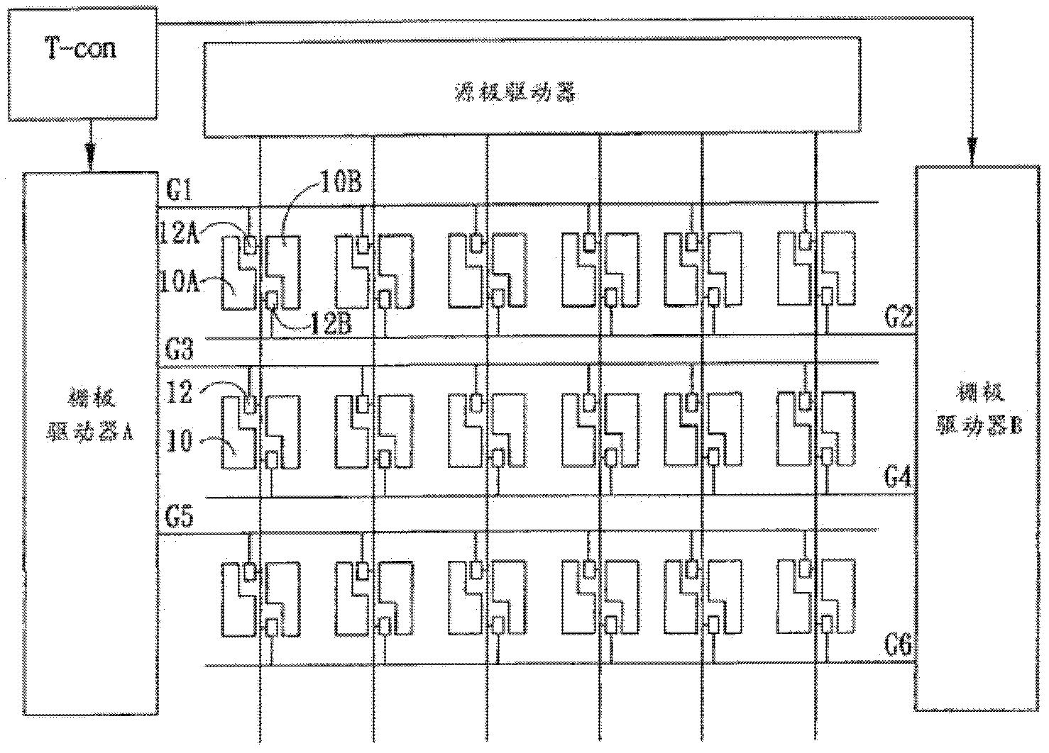
[0040] In the preparation process of the display of the present invention, in the same photolithography or mask (mask) process, the gate lead and the data line can be made on the same layer with the same material, and the gate lead passes through the via hole and the gate line. connected, so that the process can be reduced and the mask can be reduced; the gate leads can also be made on a different layer from the data lines, or not prepared in the same process, so that the gate leads and the data lines can be overlapped in the direction perpendicular to the substrate Arrangement can effectively increase the aperture ratio. It will not be described in detail here, nor should it be used as a limitation on the technical solution of the present invention.

[0041] The present invention also discloses a display device comprising the above-mentioned array substrate. The display device may include: a liquid crystal panel, a liquid crystal television, a liquid crystal display device, ...

Embodiment 1

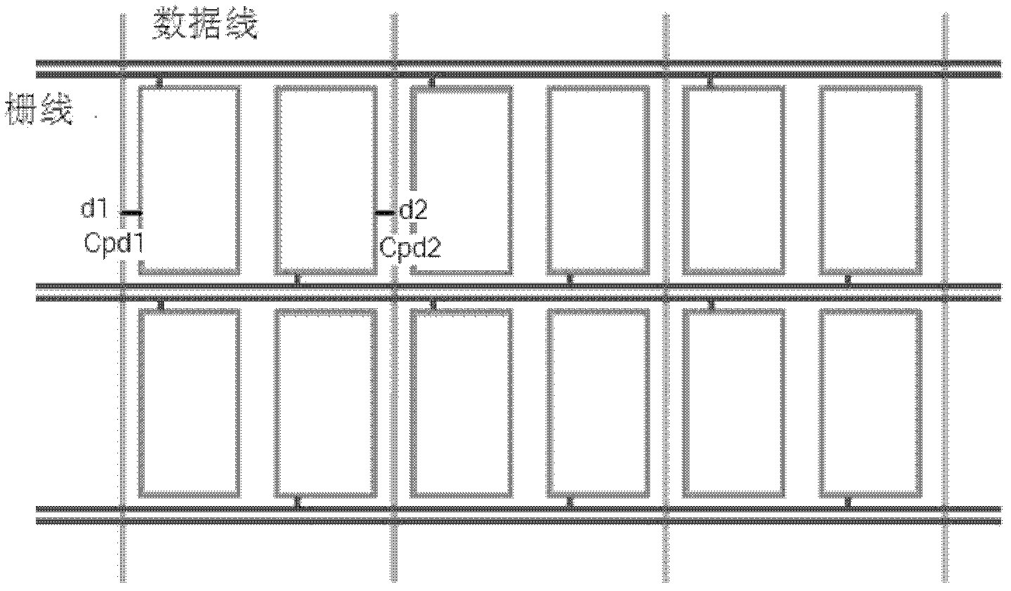
[0043] In this embodiment, a QVGA display is taken as an example. The resolution of the display is 320×240 (RGB), that is, the substrate includes 320 gate lines and 240×3=720 data lines. According to the method of the present invention, using the Dual Gate technology, the number of gate lines is doubled to 640, and correspondingly, the number of gate leads is also 640, corresponding to the gate lines one by one, while the number of data lines is halved to 360. Such as image 3 In the pixel arrangement, each gate lead is electrically connected to a gate line through a GI hole, and two gate leads are arranged between two columns of pixel units between every two data lines, that is, every two gate leads are connected to If one data line is arranged in a staggered manner, all the gate leads have been arranged after the 320th data line. In order to ensure the balance of the influence of the data lines on the pixels, two gate leads should be placed in the middle of the next 40 data ...

Embodiment 2

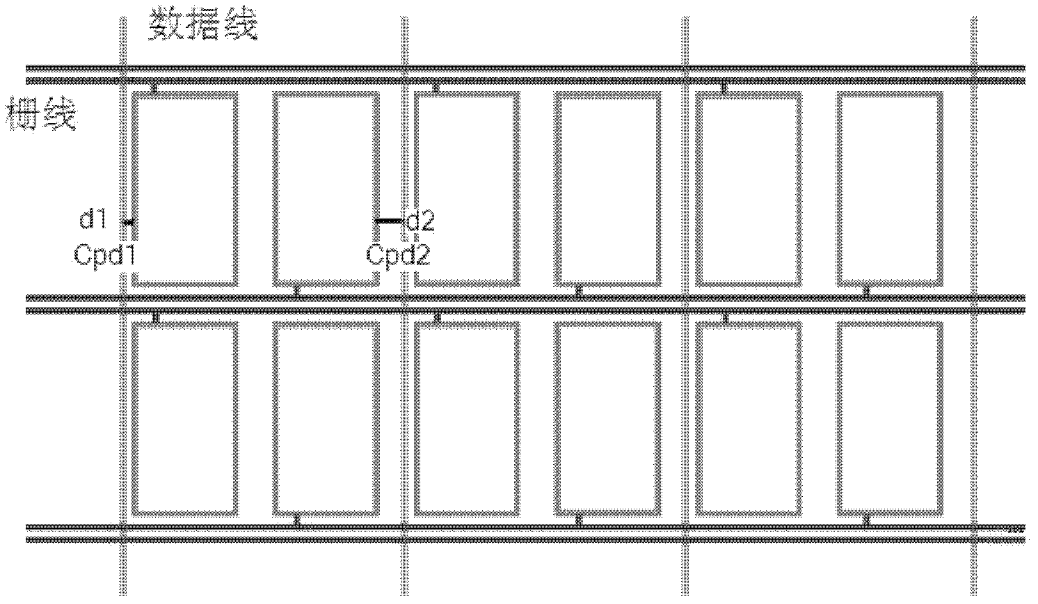
[0046] In this embodiment, a QCIF display is taken as an example. The resolution of the display is 176×144 (RGB), that is, the substrate includes 176 gate lines and 144×3=432 data lines. According to the method of the present invention, using the Dual Gate technology, the number of gate lines is doubled to 352. Correspondingly, the number of gate leads is also 352, corresponding to the gate lines one by one, while the number of data lines is halved to 216. Arrange two gate leads between 80 groups of two-column pixel units between any two data lines, and arrange two gate leads between the remaining 136 groups of two-column pixel units, which can complete 352 lead wires. Layout effect, each gate lead is electrically connected to a gate line through a GI hole, and there is no need to set a dummy line. Without setting the Dummy line, the aperture ratio of the unit pixel unit can be enlarged to improve the utilization rate of light.


PUM


Abstract

The invention discloses an array substrate and a display device, and relates to the technical field of TFT-LCDs (Thin Film Transistor Liquid Crystal Display). The array substrate comprises an active pixel region and a terminal region; the active pixel region comprises pixel units, grid lines, data lines and grid electrode leads; and two rows of pixel units are arranged between each two adjacent data lines. The array substrate is characterized in that each grid electrode lead is arranged between each two rows of pixel units; the grid electrode leads are correspondingly connected with the grid lines. According to the array substrate and the display device comprising the same, which are disclosed by the invention, the grid electrode leads are arranged in the active pixel region, so that the unbalanced influence of the data lines on pixels can be balanced and a border is narrowed.

Description

technical field [0001] The present invention relates to the technical field of Thin Film Transistor Liquid Crystal Display (TFT-LCD), in particular to a narrow frame array substrate and a display device including the array substrate. Background technique [0002] TFT-LCD has the characteristics of small size, low power consumption, and no radiation, and occupies a dominant position in the current flat panel display market. [0003] Generally speaking, the active pixel area (display area) on the TFT-LCD substrate includes a plurality of active pixel units, and each pixel unit is a rectangular area formed by the crossing of two gate lines and two data lines. TFT and a pixel electrode, the gate and source of each TFT are respectively connected to the gate line and the data line, all the gate lines are connected to the gate driver, and the data line is connected to the source driver to serve as the gate and source of the TFT Pole provides a drive signal. [0004] Since the cos...

Claims


Application Information

Patent Timeline
IPC IPC(8): G02F1/1362H01L27/02
CPCG02F2001/136231G02F2001/13456G02F2201/506G09G2310/0281G09G3/3648G09G3/00G09G2300/0426H01L27/156G02F1/136286G02F2201/40G02F2001/13606G02F1/13456G02F1/13606G02F1/136231
Inventor 王本莲张智钦白峰
Owner BOE TECH GRP CO LTD
Why Eureka
Try Eureka