


Quick Research
Generate reliable direction feasibility study reports for your R&D in just a few steps.

Technical Q&A
Discover and master advanced knowledge NOW. Basics, ideas, possibilities, all at once.

Find Solutions
As an expert in R&D theories, this can generate solutions to your technical problems instantly.

Evaluate Feasibility
Analyze your overall solution with one click, know your potential R&D risks in advance.

Monitor Landscape
Get weekly tech updates, stay abreast of the latest tech innovations and key insights.
DMOS transistor with optimized periphery structure
A technology of transistors and dielectric structures, applied in the field of DMOS transistors with optimized edge structures
- Summary
- Abstract
- Description
- Claims
- Application Information
AI Technical Summary
Problems solved by technology
Method used
Image

Examples
Embodiment Construction
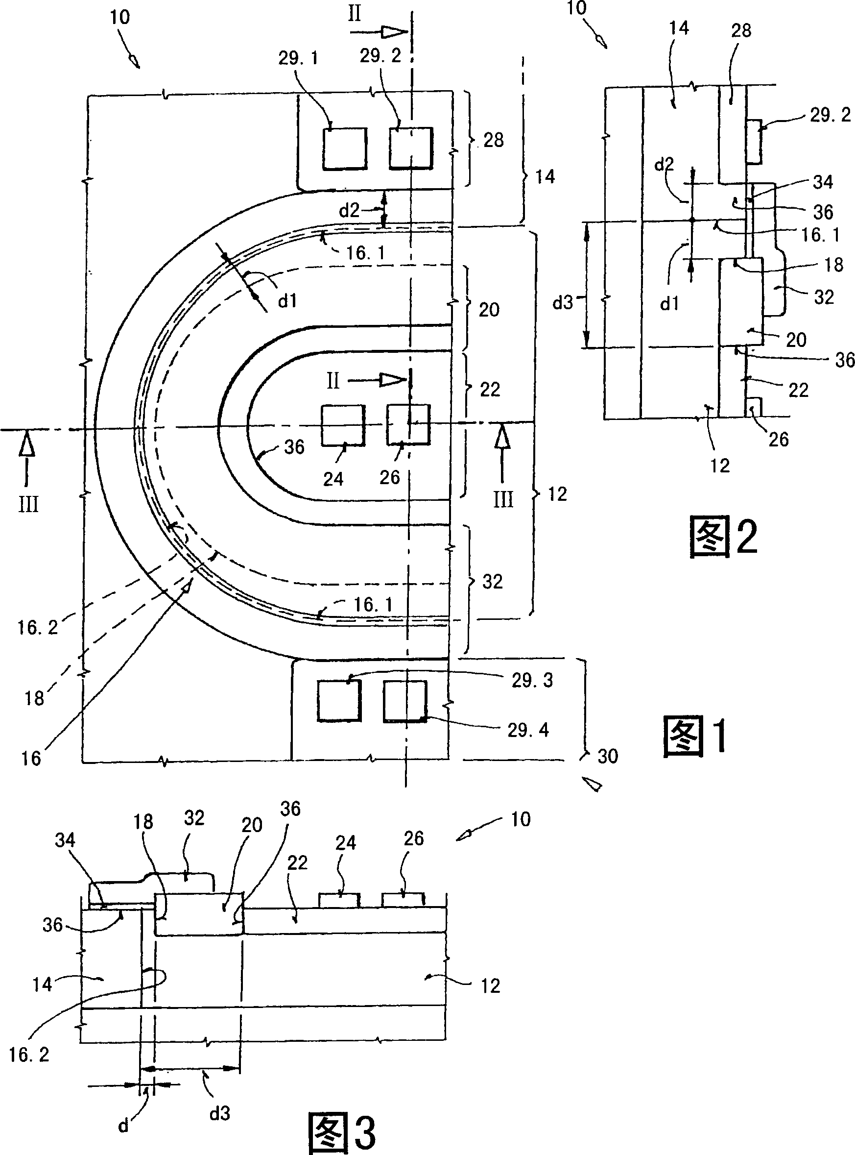
[0024] FIG. 1 shows in detail the left half of a lateral DMOS transistor 10 , which has straight and curved regions, which together give a shape reminiscent of that of a stadium or stadium track. The first region 12 composed of a semiconductor material of the first conductivity type forms an inner region which is laterally surrounded by an outer second region 14 composed of a semiconductor material of the second conductivity type. This is also illustrated by FIGS. 2 and 3 . In the schematic diagrams of FIGS. 1 to 3 , the semiconductor material of the first conductivity type has p-type conductivity, and the semiconductor material of the second conductivity type has n-type conductivity. A boundary line 16 indicated in dashed lines in FIG. 1 marks the boundary between the first region 12 and the second region 14 . The boundary line 16 here has a straight section 16.1 and a curved section 16.2.
[0025] A further dashed line marks the outer boundary 18 of the first dielectric st...
PUM
 Abstract
Description
Claims
Application Information
 - R&D Engineer
- R&D Manager
- IP Professional
- Industry Leading Data Capabilities
- Powerful AI technology
- Patent DNA Extraction
Browse by: Latest US Patents, China's latest patents, Technical Efficacy Thesaurus, Application Domain, Technology Topic, Popular Technical Reports.
© 2024 PatSnap. All rights reserved.Legal|Privacy policy|Modern Slavery Act Transparency Statement|Sitemap|About US| Contact US: help@patsnap.com