
Method for fabricating micro-electro-mechanical system (MEMS) device

a technology of micro-electromechanical systems and devices, applied in semiconductor electrostatic transducers, instruments, fluid pressure measurement, etc., can solve the problems of not being popular, not easy to integrate into the standard mos (metal-oxide semiconductor) process, and performance for current technology, etc., and achieve the effect of convenient integration

Active Publication Date: 2010-03-25
SOLID STATE SYST
View PDF16 Cites 60 Cited by
  • Summary
  • Abstract
  • Description
  • Claims
  • Application Information

AI Technical Summary

Benefits of technology

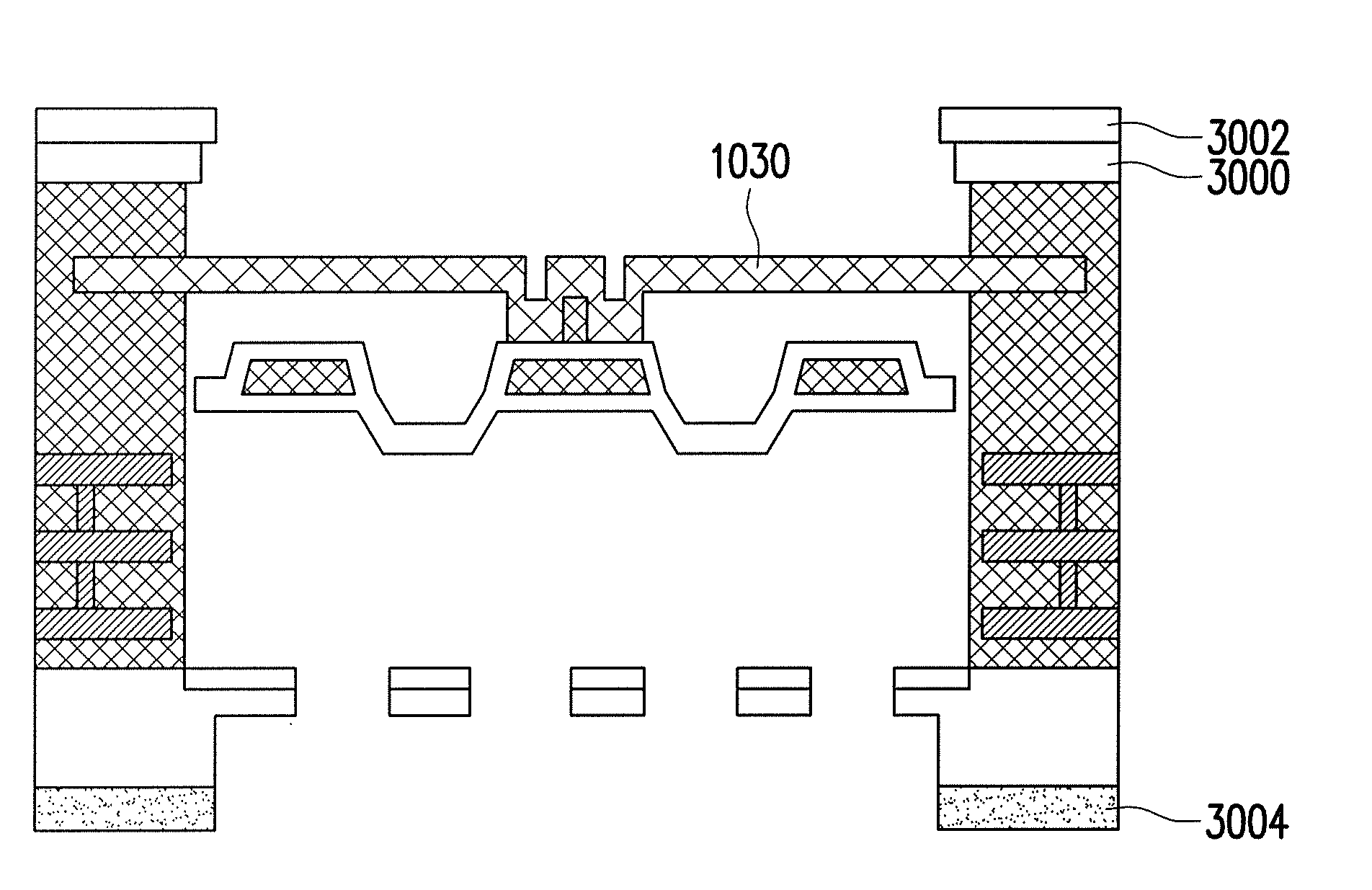
[0007]The invention provides a stress free diaphragm MEMS device and a method for fabricating the stress free diaphragm MEMS structure, in which the fabrication process can be compatible between the CMOS and MEMS device. The MEMS device can thereby be compactly integrated with the CMOS device.

Problems solved by technology

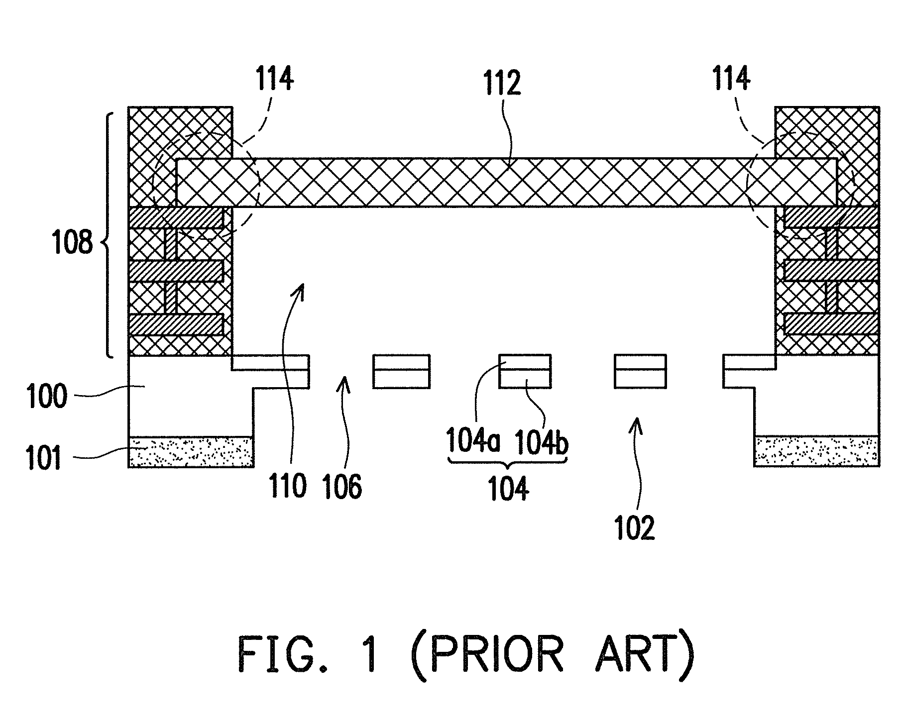
However, it is still not easy to be integrated into the standard MOS (metal-oxide semiconductor) process, such as complementary MOS (CMOS) device.
However, the cost and performance for current technology cause not being popular.
The temperature expansion coefficient and crystal mismatch of the diaphragm material and supporting frame will cause to residual stress existing in the diaphragm.
This cause the poor sensitivity, for example.

Method used


Image

  • Method for fabricating micro-electro-mechanical system (MEMS) device
  • Method for fabricating micro-electro-mechanical system (MEMS) device
  • Method for fabricating micro-electro-mechanical system (MEMS) device

Examples


Embodiment Construction

[0059]The present invention provides the MEMS structure and method for fabrication MEMS device, in which the MEMS device has the diaphragm being much free for vibration. The sensitivity can be improved. In application for MEMS microphone, the diaphragm can be more sensitivity to the acoustic signal, for example. Several embodiments are provided for description of the invention. The present invention is not just limited to the embodiments. Further, for the provided embodiments, the embodiments can be properly combined to each other without limiting to an individual embodiment itself.

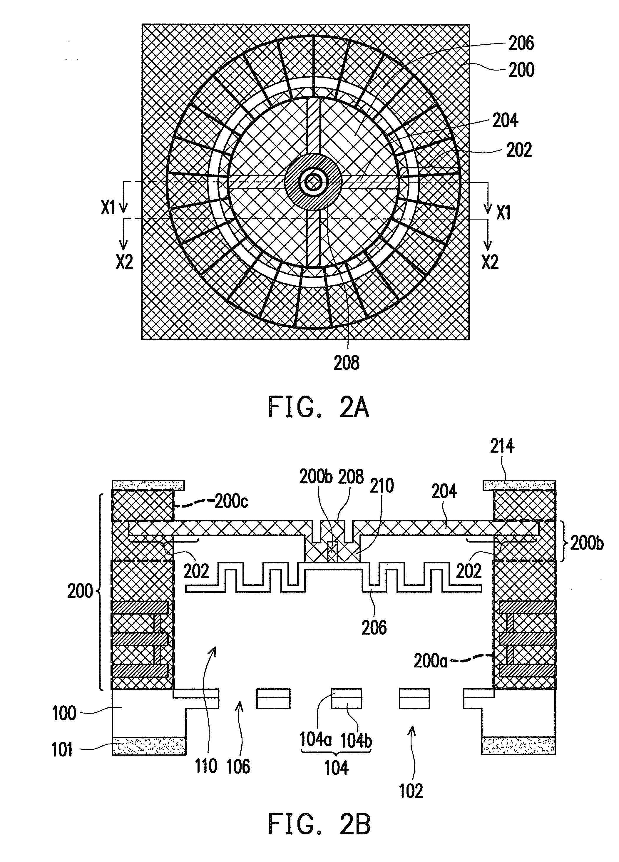
[0060]FIG. 2A is a top view, schematically illustrating a MEMS device, according to an embodiment of the present invention. FIGS. 2B and 2C are cross-sectional views, schematically illustrating the MEMS device in FIG. 2A at cutting lines X1 and X2.

[0061]Referring to FIG. 2A and FIGS. 2B-2C, the element of substrate 100, the cavity 102, the venting hole 106 and the chamber 110 are the same as in FIG. 1, an...


PUM


Abstract

A micro-electro-mechanical system (MEMS) device includes a substrate, having a first side and second side, the second side has a cavity and a plurality of venting holes in the substrate at the second side with connection to the cavity. However, the cavity is included in option without absolute need. A structural dielectric layer has a dielectric structure and a conductive structure in the dielectric structure. The structural dielectric layer has a chamber in connection to the cavity by the venting holes. A suspension structure layer is formed above the chamber. An end portion is formed in the structural dielectric layer in fix position. A diaphragm has a first portion of the diaphragm fixed on the suspension structure layer while a second portion of the diaphragm is free without being fixed.

Description

BACKGROUND OF THE INVENTION[0001]1. Field of Invention[0002]The present invention relates to a micro-electro-mechanical system (MEMS) technology with semiconductor fabrication technology. More particularly, the present invention relates to a method for fabricating a MEMS device.[0003]2. Description of Related Art[0004]MEMS devices have been widely fabricated using semiconductor fabricating process. However, it is still not easy to be integrated into the standard MOS (metal-oxide semiconductor) process, such as complementary MOS (CMOS) device. In general, a discrete MEMS device and a CMOS ASIC chip are packaged to a single die for application. However, the cost and performance for current technology cause not being popular. It is intended to develop a CMOS MEMS technology, so that the process for fabricating the MEMS can be compatible with the process for fabricating the CMOS device.[0005]MEMS Condenser Device consists of a stiff Backplate and a compliant diaphragm. Conventional the ...

Claims


Application Information

Patent Timeline
Patent Type & Authority Applications(United States)
IPC IPC(8): H01L29/84H01L21/311H01L21/00
CPCB81B2201/0257B81B2203/0127B81C1/00182B81C1/00246B81C2203/0735H01L29/84H04R19/005H04R19/04H04R31/003B81C2203/0714
Inventor LEE, CHIEN-HSINGHSIEH, TSUNG-MIN
Owner SOLID STATE SYST
Learn More