Semiconductor device with air gap and method for fabricating the same

a technology of air gap and semiconductor device, which is applied in the direction of semiconductor device details, semiconductor/solid-state device devices, electrical apparatus, etc., can solve the problems of parasitic capacitance increase, conductive structure decrease, and performance degradation of semiconductor device, so as to reduce parasitic capacitance (cb), reduce parasitic capacitance reduce sheet resistance (rs) of conductive structure, the effect of reducing the resistan

Active Publication Date: 2015-01-15
SK HYNIX INC
View PDF6 Cites 60 Cited by
  • Summary
  • Abstract
  • Description
  • Claims
  • Application Information

AI Technical Summary

Benefits of technology

[0018]Additionally, since conductive structures include a silicide layer, the sheet resistance (Rs) of the conductive structures may be reduced. In particular, since a low resistance silicide layer is included, the sheet resistance (Rs) of the conductive structures may be further reduced. As the sheet resistance (Rs) is reduced, a contact resistance (Rc) may be improved.
[0019]Further, since a contact area increases as an ohmic contact layer covers a silicon plug, the contact resistance (Rc) of the conductive structures may be further improved. Moreover, it is possible to cap the air gaps using a conductive material without using a dielectric material. As a consequence, a parasitic capacitance (Cb) may be reduced due to the air gaps, a sheet resistance (Rs) may be reduced by the low resistance silicide layer, and the contact resistance (Rc) of the conductive structures may be improved attributable to an increase in contact area.

Problems solved by technology

As a semiconductor device is highly integrated, a distance between conductive structures is gradually decreasing, thus, parasitic capacitance increases.
As parasitic capacitance increases, the performance of the semiconductor device is degraded.
However, since the dielectric material has a high dielectric constant, limitations may exist in reducing parasitic capacitance.

Method used


Image

  • Semiconductor device with air gap and method for fabricating the same
  • Semiconductor device with air gap and method for fabricating the same
  • Semiconductor device with air gap and method for fabricating the same

Examples


first embodiment

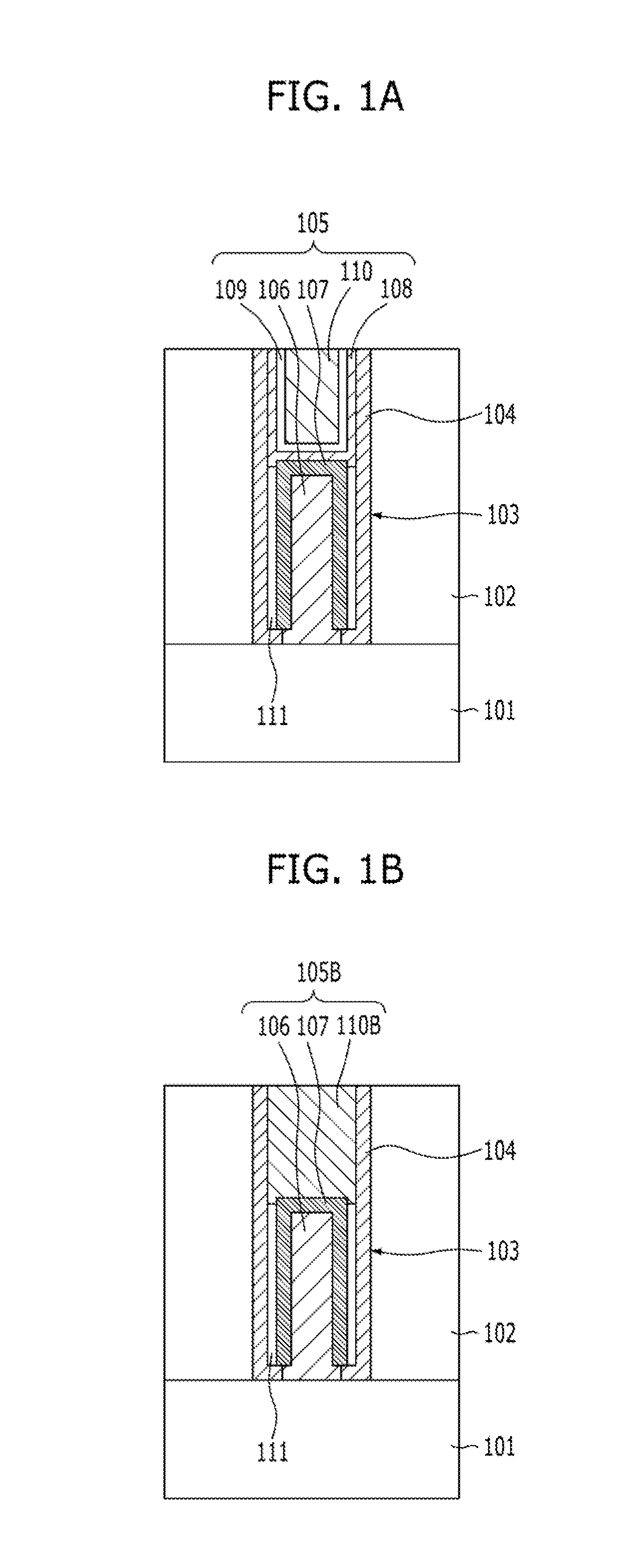
[0045]FIG. 1A is a cross-sectional view illustrating a semiconductor device in accordance with a

[0046]Referring to FIG. 1A, a dielectric layer 102 is formed on a substrate 101. An opening 103 is defined in the dielectric layer 102 to expose the surface of the substrate 101. A conductive structure 105 is formed in the opening 103. The conductive structure 105 includes a first conductive pattern 106 and a third conductive pattern 110. The third conductive pattern 110 is formed over the first conductive pattern 106. A second conductive pattern 107 is formed between the first conductive pattern 106 and the third conductive pattern 110. The second conductive pattern 107 covers the top surface and the sidewalls of the first conductive pattern 106. A barrier pattern 108 and a glue pattern 109 are formed between the second conductive pattern 107 and the third conductive pattern 110. An air gap 111 is defined between the second conductive pattern 107 and the sidewalls of the opening 103. The...

second embodiment

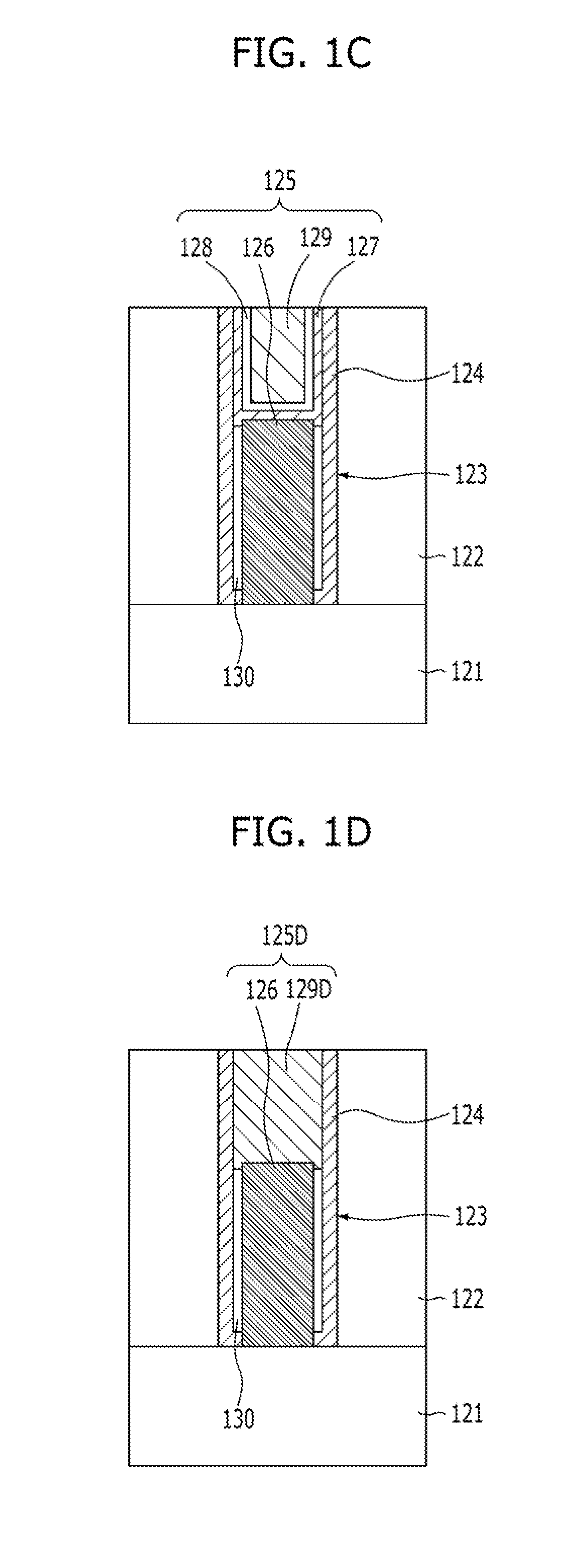
[0058]FIG. 1C is a cross-sectional view illustrating a semiconductor device in accordance with a

[0059]Referring to FIG. 1C, a dielectric layer 122 is formed on a substrate 121. An opening 123 is defined in the dielectric layer 122 to expose the surface of the substrate 121. A conductive structure 125 is formed in the opening 123. The conductive structure 125 includes a first conductive pattern 126 and a second conductive pattern 129. The second conductive pattern 129 is formed over the first conductive pattern 126. A barrier pattern 127 and a glue pattern 128 are formed between the first conductive pattern 126 and the second conductive pattern 129. An air gap 130 is defined between the first conductive pattern 126 and the sidewalls of the opening 123. The barrier pattern 127 caps the air gap 130 and covers the top surface and the sidewalls of an upper portion of the first conductive pattern 126. A spacer 124 may be formed on the sidewalls of the opening 123.

[0060]The first conductiv...

third embodiment

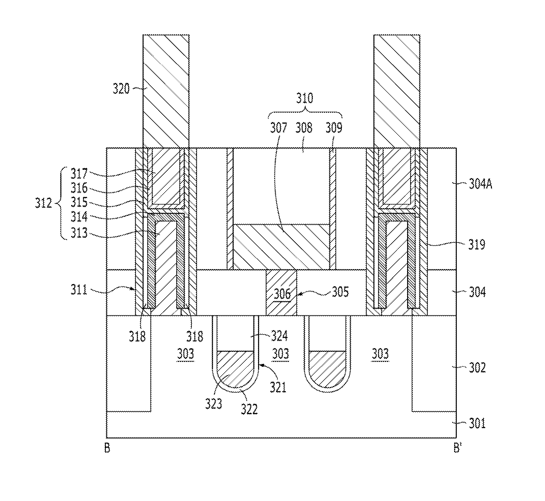
[0111]FIG. 6A is a cross-sectional view illustrating a semiconductor device in accordance with a

[0112]Referring to FIG. 6A, a plurality of conductive structures are formed on a substrate 201. The conductive structures include first conductive structures 204 and second conductive structures 205. Dielectric structures with air gaps 209 are formed between the first conductive structures 204 and the second conductive structures 205. Spacers 210 are formed on the sidewalls of the first conductive structures 204. The air gaps 209 are defined between the spacers 210 and the second conductive structures 205. Each of the first conductive structures 204 includes a first conductive pattern 202 and a dielectric pattern 203. Each of the second conductive structures 205 includes a second conductive pattern 206, a third conductive pattern 207, a barrier pattern 211, a glue pattern 212, and a fourth conductive pattern 208. The third conductive patterns 207 and the air gaps 209 are capped by the bar...


PUM


Abstract

A semiconductor device includes a dielectric structure which has an opening exposing a surface of a substrate; and a conductive structure which is formed in the opening, wherein the conductive structure comprises: a first conductive pattern recessed in the opening; a second conductive pattern covering a top surface and sidewalls of the first conductive pattern; an air gap defined between sidewalls of the opening and the second conductive pattern; and a third conductive pattern capping the second conductive pattern and the air gap.

Description

CROSS-REFERENCE TO RELATED APPLICATIONS[0001]The present application claims priority of Korean Patent Application No. 10-2013-0081885, filed on Jul. 12, 2013, which is incorporated herein by reference in its entirety.BACKGROUND[0002]1. Field[0003]Exemplary embodiments of the present invention relate to a semiconductor device, and more particularly, to a semiconductor device with air gaps and a method for fabricating the same.[0004]2. Description of the Related Art[0005]In general, in a semiconductor device, a dielectric material is formed between adjacent conductive structures. As a semiconductor device is highly integrated, a distance between conductive structures is gradually decreasing, thus, parasitic capacitance increases. As parasitic capacitance increases, the performance of the semiconductor device is degraded.[0006]To reduce parasitic capacitance, the dielectric constant of a dielectric material may be decreased. However, since the dielectric material has a high dielectric ...

Claims


Application Information

Patent Timeline
Patent Type & Authority Applications(United States)
IPC IPC(8): H01L23/532H01L21/768H01L23/528H01L27/108H01L23/522
CPCH01L27/10876H01L27/10855H01L23/528H01L23/5329H01L27/10885H01L23/53266H01L21/7682H01L23/5222H01L27/10814H01L23/53271H01L23/53295H01L2924/0002H01L21/76897H01L23/485H01L21/76831H01L21/76889H10B12/315H10B12/053H10B12/0335H10B12/482H01L2924/00H01L21/764H10B99/00H10B12/00H10B12/34H01L21/76895H01L21/76816H01L21/76843H01L21/76877H01L23/5226
Inventor LEE, NAM-YEALYEOM, SEUNG-JIN
Owner SK HYNIX INC
Why Eureka
Try Eureka