Gas wall electrode side connection phase shift storage and its producing method

A manufacturing method and phase change technology, applied in semiconductor/solid-state device manufacturing, electric solid-state devices, circuits, etc., can solve problems such as power consumption, increase in parasitic resistance, component uniformity and reliability, etc.

Inactive Publication Date: 2007-06-27
IND TECH RES INST
View PDF0 Cites 5 Cited by
  • Summary
  • Abstract
  • Description
  • Claims
  • Application Information

AI Technical Summary

Problems solved by technology

Generally speaking, in order to increase the heating efficiency of the phase change material, the heating electrode material used in the phase change memory usually needs to have a higher resistivity, and if the heating electrode is also used as a wire in the design, it will be Make the parasitic resistance of the component increase and cause additional power consumption
Furthermore, when the distance between the two electrodes is gradually reduced, it will cause difficulties for the phase change material to fill holes, which will lead to poor interface contact between the side contact electrodes and the phase change material, which will easily cause problems in the uniformity and reliability of the components.

Method used


Image

  • Gas wall electrode side connection phase shift storage and its producing method
  • Gas wall electrode side connection phase shift storage and its producing method
  • Gas wall electrode side connection phase shift storage and its producing method

Examples


Embodiment Construction

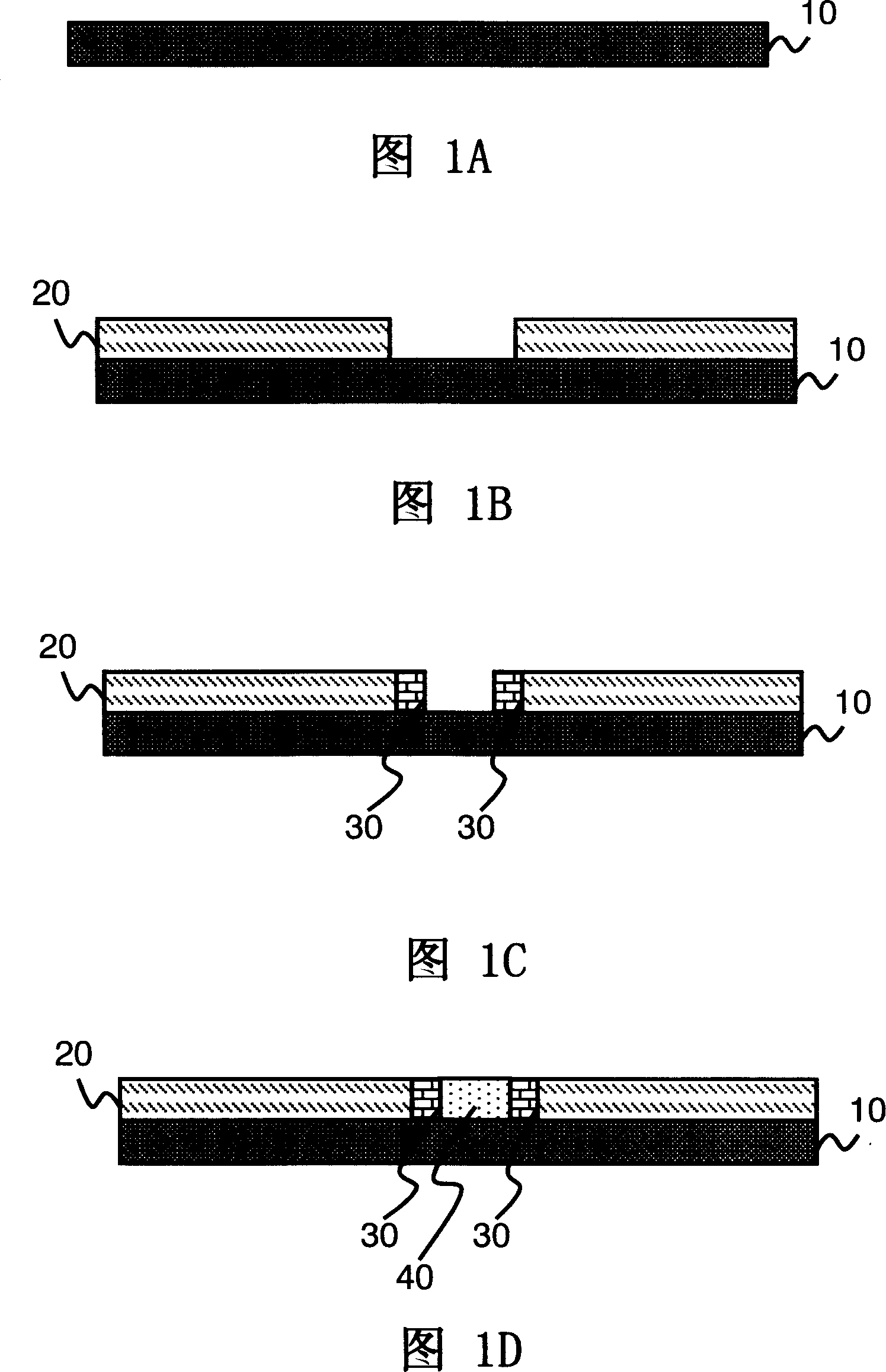
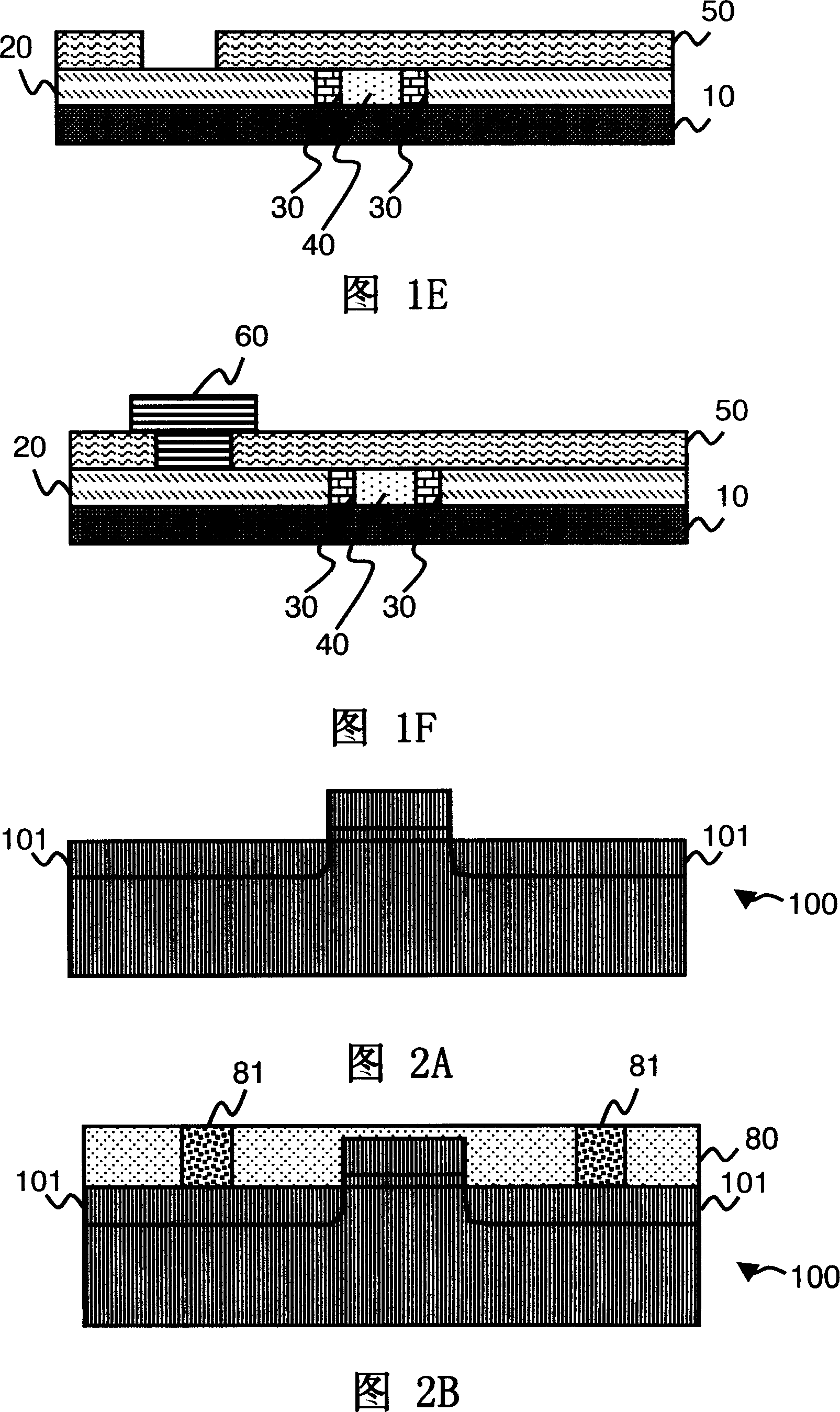
[0037] In the known phase change memory, the conductive region and the phase change material layer 40 are stacked on each other, the phase change material layer 40 is parallel to the surface of the substrate, and one or more channels pass through the insulating layer to expose the conductive region. The area of ​​the channel is used to determine the electrical contact area between the conductive region and the phase change material layer 40 , and the plane of the contact region is parallel to the substrate. The minimum size of the channel (i.e. the minimum contact area) is mainly determined by the photolithography process, and the area of ​​the channel will determine the operating current flowing vertically into the phase change material layer 40, which is to determine whether to set or reset the phase change material layer 40. Therefore, in the known practice, the operating current of the phase change memory is mainly limited by the capability of the photolithography process. ...


PUM


Abstract

This invention discloses a clearance wall electrode side connected phase change memory and its manufacturing method including applying a conductor electrode with rather low resistivity to combine with clearance wall electrode of high resistivity and forming the phase change material layer between the clearance wall electrodes so as to reduce the contact area between the phase change material layer and the wall electroce and reduce the volume of the material to further reduce the operation current and power loss of the phase change memory.

Description

technical field [0001] The present invention relates to a phase change memory, in particular to a spacer electrode side-connected phase change memory and its manufacturing method in which electrodes with a smaller contact area are formed in the phase change memory to reduce the operating current required for phase change. Background technique [0002] Many different materials have two or more states, and materials with two states are especially suitable for digital memory. These materials can produce a thermally induced transition phenomenon with temperature changes, and present an amorphous state or a crystalline state. [0003] Basically, when the material is in an amorphous state (with an irregularly arranged atomic structure), it will exhibit high resistivity; while when the material is in a crystalline state (with a neatly arranged atomic structure), it will exhibit low resistivity. The amorphous state or reset state can represent a logical state of 1, while the crysta...

Claims


Application Information

Patent Timeline
Patent Type & Authority Applications(China)
IPC IPC(8): H01L45/00H01L27/24H01L21/82
Inventor 赵得胜王文翰李敏鸿许宏辉李乾铭卓言陈颐承陈维恕
Owner IND TECH RES INST
Why Eureka
Try Eureka