Semiconductor element with semiconductor component embedded into a plastic housing

A technology for structural components and plastic housings, applied in the fields of semiconductor/solid-state device parts, semiconductor devices, semiconductor/solid-state device manufacturing, etc., can solve the problems of high welding temperature of 260 ° C, improve reliability and prevent the spread of cracks Effect

Active Publication Date: 2007-07-11
INFINEON TECH AG
View PDF3 Cites 3 Cited by
  • Summary
  • Abstract
  • Description
  • Claims
  • Application Information

AI Technical Summary

Problems solved by technology

However, lead-free solder has the following disadvantages, that is, a higher soldering temperature of 260°C is required

Method used


Image

  • Semiconductor element with semiconductor component embedded into a plastic housing
  • Semiconductor element with semiconductor component embedded into a plastic housing

Examples


Embodiment Construction

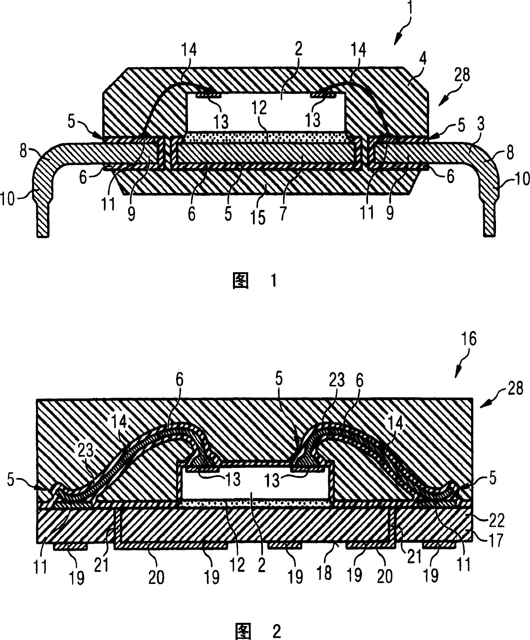
[0050] FIG. 1 shows a cross-sectional view of a semiconductor component 1 with a semiconductor chip 2 and a flat lead frame 3 . The region of the flat lead frame 3 which is embedded in the plastic housing 4 is coated with a buffer layer 5 . The buffer layer 5 is made of a thermoplastic material 6 , which is polyamide 66 in this embodiment.

[0051] The flat lead frame plus 3 has a chip island 7 and a plurality of flat wires 8 surrounding the chip island 7 . Each flat conductor has an inner region 9 embedded in the plastic housing 4 of the component 1 and an outer region 10 located outside the plastic housing 4 . The outer region 10 of the flat conductor 8 defines the external contacts of the semiconductor component, with which the semiconductor component 1 can be mounted on a printed circuit board. The inner region 9 of each flat conductor 8 has an inner contact surface 11 . The flat leadframe 3 has Cu and the inner contact surface 11 has a Ni / NiP layer.

[0052] The inert...


PUM


Abstract

A semiconductor device includes semiconductor device components embedded in plastic package compound, with a buffer layer being arranged on surfaces of the semiconductor device components of the semiconductor device. The buffer layer includes a thermoplastic material.

Description

technical field [0001] The invention relates to a semiconductor component having a semiconductor component embedded in a plastic housing, wherein the surface of the semiconductor component is at least partially provided with a buffer layer. Furthermore, the invention relates to a method for producing a semiconductor component, a system carrier and a buffer layer of this type. Background technique [0002] According to this production method, the functionality and reliability of the components are checked. Due to the increased temperature, this method can lead to the formation of cracks and even delamination at the boundaries between the different materials of the semiconductor component. Especially the formation of cracks between the circuit holder and the plastic housing is a problem. [0003] The lack of adhesion between the system carrier and the plastic housing causes moisture to collect in the boundary layer between the system carrier and the plastic housing in the se...

Claims


Application Information

Patent Timeline
Patent Type & Authority Applications(China)
IPC IPC(8): H01L23/495H01L23/28H01L23/29H01L23/31H01L23/16H01L21/48H01L21/56H01L21/54
CPCH01L24/83H01L24/85H01L2224/83H01L23/3121H01L2224/73265H01L23/3142H01L24/45H01L2224/48624H01L2224/32225H01L2924/12041H01L2924/01015H01L2224/48091H01L2924/01047H01L2224/8592H01L2924/01078H01L2924/01006H01L2924/01028H01L24/48H01L2924/01079H01L2224/32245H01L2924/14H01L2924/01024H01L2924/01005H01L2924/0103H01L2924/01082H01L23/3107H01L2224/45144H01L2924/01013H01L2924/014H01L2924/01029H01L2224/48247H01L2224/05624H01L2224/48465H01L2224/48227H01L2924/01033
Inventor J·马勒S·M·汤
Owner INFINEON TECH AG
Why Eureka
Try Eureka