
Apparatus and sensor chip component attaching method

a technology of attaching method and sensor chip, which is applied in the direction of electrical equipment, basic electric elements, instruments, etc., can solve the problems of contaminating the optical surface of the lens, becoming more difficult to use a conventional scheme for attaching adhesive between the lens and the sensor, etc., and achieves the effect of effective and efficient application

Active Publication Date: 2018-07-17
PIXART IMAGING PENANG
View PDF14 Cites 0 Cited by
  • Summary
  • Abstract
  • Description
  • Claims
  • Application Information

AI Technical Summary

Benefits of technology

The present invention provides an apparatus and method for attaching a sensor chip component to an integrated circuit package using adhesive material. This method effectively and efficiently distributes the adhesive material without contaminating surfaces that need to stay clean. This is particularly useful for small products where the risk of contamination is higher. Overall, this method improves the attachment speed and reliability of the sensor chip component to the integrated circuit package.

Problems solved by technology

However, it becomes more difficult to use a conventional scheme for applying the adhesives between the lens and sensor since the size of the components in miniature optical navigation systems becomes smaller.
The conventional scheme usually runs the risk of contaminating the optical surfaces of the lens in the process.

Method used


Image

  • Apparatus and sensor chip component attaching method
  • Apparatus and sensor chip component attaching method
  • Apparatus and sensor chip component attaching method

Examples


Embodiment Construction

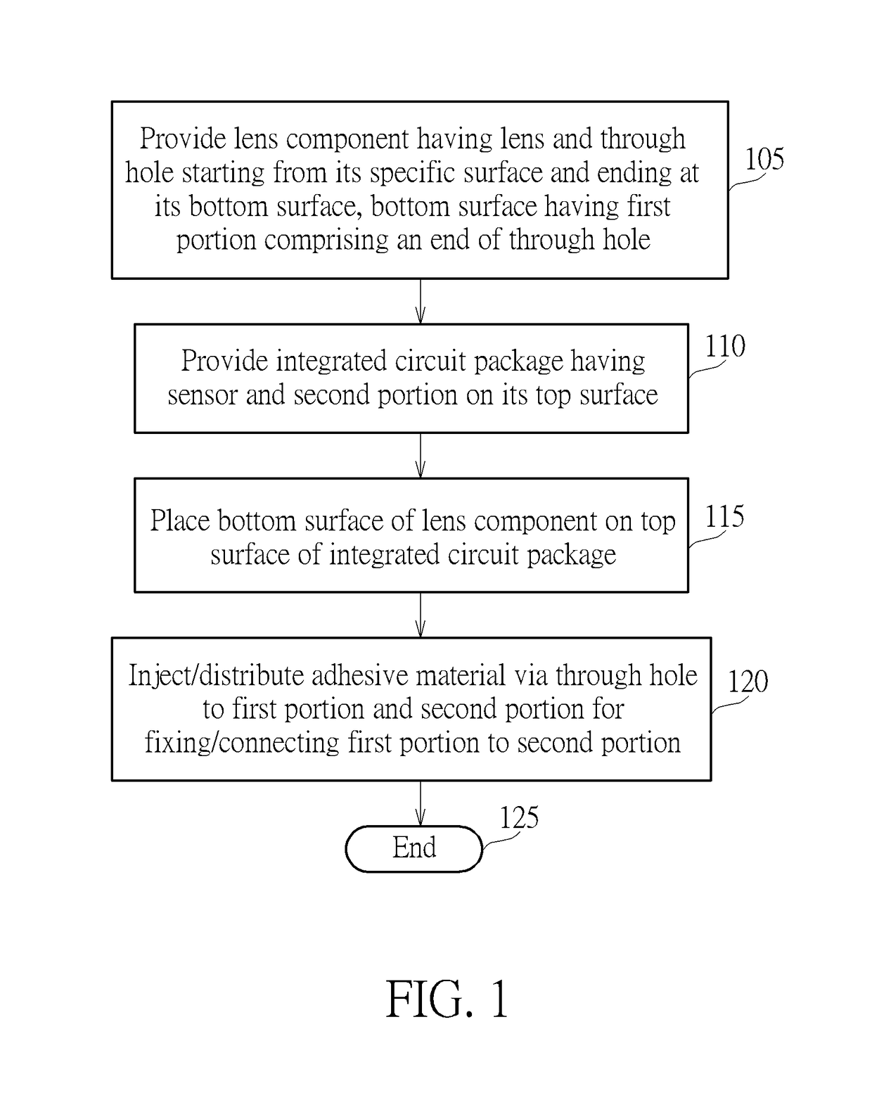
[0017]Please refer to FIG. 1, which is a diagram illustrating a flowchart of a sensor chip component attaching / assembling method according to embodiments of the present invention. In the embodiments, the attaching / assembling method is used for attaching / fixing a lens component / circuit to an integrated circuit package having a sensor. It should be noted that this attaching / assembling method can be also applied for any kinds of chip packages for attaching / fixing a specific component to an integrated circuit package, not limited to attaching a lens component to a sensor circuit package. Provided that substantially the same result is achieved, the steps of the flowchart shown in FIG. 1 need not be in the exact order shown and need not be contiguous, that is, other steps can be intermediate. The description of steps is detailed in the following:

[0018]Step 105: Provide a lens component having a lens and a through hole wherein the through hole starts from a specific surface and ends at a b...


PUM


Abstract

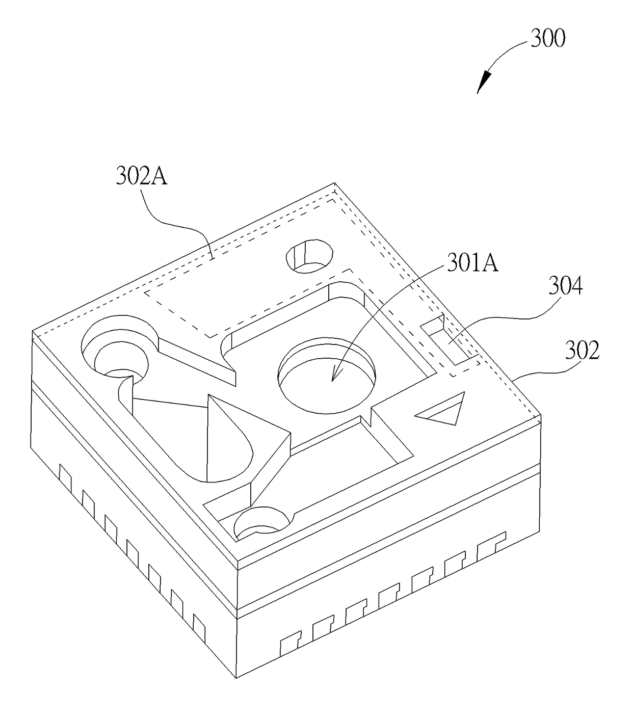
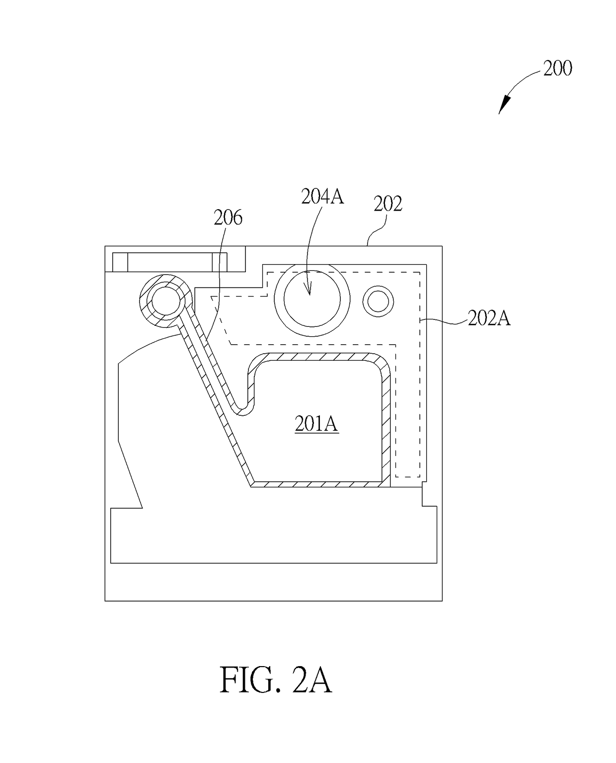
An apparatus includes a lens component and an integrated circuit package. The lens component has a lens and a through hole from a specific surface to a bottom surface of the lens component. The integrated circuit package has a sensor and a second portion on a top surface of the integrated circuit package. The first portion on the bottom surface of the lens component is adjacent and attached to the second portion on the top surface of the integrated circuit package by an adhesive material that is injected via the through hole to the first portion and the second portion, for fixing the lens component to the integrated circuit package.

Description

BACKGROUND OF THE INVENTION[0001]1. Field of the Invention[0002]The present invention relates to a circuit component attaching scheme, and more particularly to an apparatus and a sensor chip component attaching method.[0003]2. Description of the Prior Art[0004]Generally speaking, a conventional optical navigation system consists of a sensor mated with a lens and potentially a holder or bracket. The component (i.e. lens to sensor) attachment process and mechanism in current products may involve a conventional mechanical fitting scheme. The use of conventional mechanical fitting scheme has the advantage of simple assembly but still needs to provide for strong and more permanent adhesives between the lens and sensor. The use of adhesives enables strong and permanent attachment to be achieved. However, it becomes more difficult to use a conventional scheme for applying the adhesives between the lens and sensor since the size of the components in miniature optical navigation systems beco...

Claims


Application Information

Patent Timeline
Patent Type & Authority Patents(United States)
IPC IPC(8): H01L31/0232H01L21/8222H01L27/146G02B7/02G02B27/00
CPCH01L27/14627H01L27/14685G02B27/0006G02B7/025
Inventor T'NG, CHEE PINLEE, SAI MUN
Owner PIXART IMAGING PENANG
Learn More